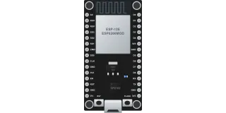
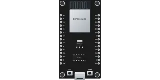
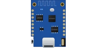
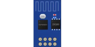
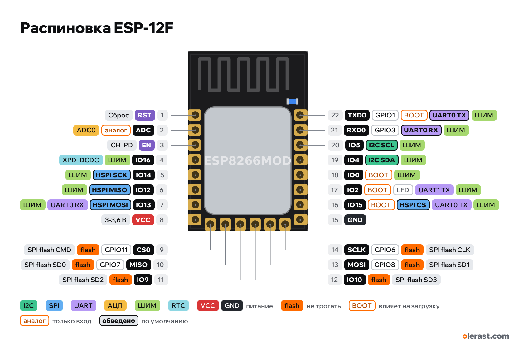
ESP-12F pinout
ESP-12F (Ai-Thinker), ESP8266EX, 3.3 V logic, 16×24 mm, 22 pins
verified20.10.2026
Top view (shield side), antenna at the top.
CompareDownload PNG- Chip
- ESP8266EX
- Logic
- 3.3 V
- Power
- VCC 3-3.6 V
- Defaults in ESP8266 Arduino core (NodeMCU 1.0, ESP-12E Module)
- I2C: SDA 4, SCL 5SPI: MOSI 13, MISO 12, SCK 14, SS 15UART: TX 1, RX 3LED: 2
Which ESP-12F pins are safe to use
Free to use
GPIO3-5, GPIO12-14, GPIO16
Use with care
- GPIO0, GPIO2, GPIO15: strapping: the level at power-up selects the boot mode.
- GPIO1: signal at boot.
- A0: analog input only.
Leave alone
- GPIO6-11: flash and PSRAM memory.
Important
- 3.3 V only for supply and signals.
- Boot circuit: EN and RST to 3.3 V through 10 kΩ, GPIO15 to GND through 10 kΩ, GPIO0 and GPIO2 to 3.3 V through 10 kΩ.
- Flashing: GPIO0 to GND at power-up or reset, TXD0 and RXD0 crossed to a USB-UART adapter.
- The module draws up to 170 mA when transmitting: power it from a regulator rated 500 mA or more, with 10 µF and 100 nF capacitors at VCC.
- The bottom row (CS0, MISO, IO9, IO10, MOSI, SCLK) is wired to the module's flash: connect nothing.
- ADC: 0-1.0 V, no divider on the module.
- To wake from deep sleep, connect IO16 to RST.
- Pin numbers 1-22 follow the Ai-Thinker application circuit. In table 2.2 of the same specification the 16 side pins are numbered differently: from 9 GND to 16 TXD up the right edge.
- Pin labels are printed on the back of the module; the shield covers them on top.
- Ai-Thinker: power source rated 500 mA or more, a separate DC-DC or LDO.
- Do not apply 5 V to VCC or the pins.
Revisions and clones
- ESP-12E: same pinout and size, different antenna shape.
- ESP-12S: 16 pins without the bottom row, pull-ups on EN, RST, GPIO0, GPIO15 are already on the module.
All pins
| Label | Number | Functions | Limits | Check |
|---|---|---|---|---|
| RST | pin 1 | Reset (low = reset) | verifiedPull up to 3.3 V through 10 kΩ to boot (Ai-Thinker application circuit). | |
| ADC | TOUT, Arduino A0, pin 2 | ADC0 (A0), 10 bit | analog input onlynot 5 V tolerant | verifiedADC input 0-1.0 V, no divider on the module.Labelled on other revisions as: TOUT, A0 |
| EN | pin 3 | CH_PD: chip enable (high = running) | verifiedPull up to 3.3 V through 10 kΩ to boot.Labelled on other revisions as: CH_PD | |
| IO16 | GPIO16, pin 4 | XPD_DCDC: wake from deep sleep (connect to RST)PWM (software) | not 5 V tolerantno interrupts | verifiedGPIO16 is in the RTC domain: no interrupts and no pull-up (only INPUT_PULLDOWN_16). To wake from deep sleep, connect it to RST.Labelled on other revisions as: GPIO16 |
| IO14 | GPIO14, pin 5 | interruptPWM (software)HSPI SCK | not 5 V tolerant | verifiedLabelled on other revisions as: GPIO14 |
| IO12 | GPIO12, pin 6 | interruptPWM (software)HSPI MISO | not 5 V tolerant | verifiedLabelled on other revisions as: GPIO12 |
| IO13 | GPIO13, pin 7 | interruptPWM (software)HSPI MOSIUART0 RX (Serial.swap) | not 5 V tolerant | verifiedLabelled on other revisions as: GPIO13 |
| VCC | pin 8 | 3.3 V | power input | verified3.0-3.6 V only. Up to 170 mA when transmitting: 10 µF and 100 nF capacitors at the pin (Ai-Thinker circuit).Labelled on other revisions as: 3V3 |
| CS0 | GPIO11, pin 9 | SPI flash CMD | not 5 V tolerantused by flash, do not use | verifiedConnected to the module flash. Do not use. |
| MISO | GPIO7, pin 10 | SPI flash SD0 | not 5 V tolerantused by flash, do not use | verifiedConnected to the module flash. Do not use. |
| IO9 | GPIO9, pin 11 | SPI flash SD2 | not 5 V tolerantused by flash, do not use | verifiedConnected to the module flash. Do not use.Labelled on other revisions as: GPIO9 |
| IO10 | GPIO10, pin 12 | SPI flash SD3 | not 5 V tolerantused by flash, do not use | verifiedConnected to the module flash. Do not use.Labelled on other revisions as: GPIO10 |
| MOSI | GPIO8, pin 13 | SPI flash SD1 | not 5 V tolerantused by flash, do not use | verifiedConnected to the module flash. Do not use. |
| SCLK | GPIO6, pin 14 | SPI flash CLK | not 5 V tolerantused by flash, do not use | verifiedConnected to the module flash. Do not use. |
| GND | pin 15 | Ground | verified | |
| IO15 | GPIO15, pin 16 | interruptPWM (software)HSPI CS (SS)UART0 TX (Serial.swap) | not 5 V tolerantaffects boot (strapping) | verifiedMust be low at reset (boards have a pull-down). Do not pull up.Pull down to GND through 10 kΩ to boot (Ai-Thinker circuit).Labelled on other revisions as: GPIO15 |
| IO2 | GPIO2, pin 17 | interruptPWM (software)UART1 TX (Serial1, transmit only) | not 5 V tolerantaffects boot (strapping)onboard LED | verifiedMust be high at reset, otherwise the board will not start.Must be high at power-up: pull-up to 3.3 V.Blue LED on the module (lit when LOW). It is not on the Ai-Thinker schematic; per the ESP8266 core LED_BUILTIN = 2.Labelled on other revisions as: GPIO2 |
| IO0 | GPIO0, pin 18 | interruptPWM (software) | not 5 V tolerantaffects boot (strapping) | verifiedAt reset: low = firmware download mode, high is needed for a normal boot.10 kΩ pull-up to 3.3 V to boot, to GND at power-up for flashing.Labelled on other revisions as: GPIO0 |
| IO4 | GPIO4, pin 19 | interruptPWM (software)I2C SDA | not 5 V tolerant | verifiedLabelled on other revisions as: GPIO4 |
| IO5 | GPIO5, pin 20 | interruptPWM (software)I2C SCL | not 5 V tolerant | verifiedLabelled on other revisions as: GPIO5 |
| RXD0 | GPIO3, pin 21 | interruptPWM (software)UART0 RX | not 5 V tolerant | verifiedUsed for UART flashing.Labelled on other revisions as: RXD, RX |
| TXD0 | GPIO1, pin 22 | interruptPWM (software)UART0 TX | not 5 V tolerantoutputs a signal at boot | verifiedPrints the bootloader log at boot (74880 baud).Labelled on other revisions as: TXD, TX |
Sources
Every pin is verified against the manufacturer's documents.
- ESP-12F Datasheet V1 (Ai-Thinker), specification 2022-08-07datasheet, checked 20.10.2026size 16×24 mm, 22 pins, 2 mm pitch, holes 1 mm from the side edges, lowest side pin 1.5 mm from the edge, bottom row x 3-13 mm; pin functions (table 2.2), boot modes (table 2.3), application circuit with numbers 1-22, 10 kΩ resistors on RST, EN, GPIO0, GPIO15, 10 µF and 100 nF capacitors, transmit current 170 mA (802.11b), deep sleep 20 µA, supply 3.0-3.6 V from 500 mA
- Ai-Thinker: ESP8266 documentation (module table)user guide, checked 20.10.2026link to the ESP-12F specification and the PCB_ESP8266 footprint
- ESP8266EX Datasheet (Espressif)datasheet, checked 15.10.2026pins and functions, TOUT (ADC 0–1.0 V), HSPI, UART0/UART1, strapping GPIO0/2/15, flash pins, GPIO16 XPD_DCDC
- ESP8266 Arduino Core: Reference (GPIO, PWM, interrupts, Serial)Arduino core, checked 15.10.2026PWM on GPIO0–16, interrupts on all except GPIO16, GPIO6–11 used by flash, Serial1 TX only on GPIO2, Serial.swap on 15/13
- esp8266/Arduino: variants/nodemcu/pins_arduino.h and common.hArduino core, checked 15.10.2026D0–D8 ↔ GPIO, SDA 4, SCL 5, SS 15, MOSI 13, MISO 12, SCK 14, LED_BUILTIN 2
Size: 24×16×3 mm (±0.2) per the Ai-Thinker specification.
FAQ
- Which ESP-12F pins are I2C, SPI and UART?
- By default in ESP8266 Arduino core (NodeMCU 1.0, ESP-12E Module): I2C: SDA GPIO4, SCL GPIO5; SPI: MOSI GPIO13, MISO GPIO12, SCK GPIO14, SS GPIO15; UART: TX GPIO1, RX GPIO3.
- Which pin is the ESP-12F LED on?
- Blue LED on GPIO2, lit when LOW (per the ESP8266 core, not shown on the schematic).
- Are the ESP-12F pins 5 V tolerant?
- No. The logic is 3.3 V and the pins are not 5 V tolerant: use a divider or a level shifter for 5 V signals.
- What supply voltage does the ESP-12F need?
- VCC: 3-3.6 V. 3.3 V logic.
You might also need
Schematic with this board
schematic builder with the board already placed
Flash this board
upload a sketch or .bin to this board from the browser
Power budget
will the regulator cope and how long the battery lasts
Calculators
LED resistor, voltage divider, battery runtime, 3D print cost, LED strip power supply and pF, nF, µF conversion