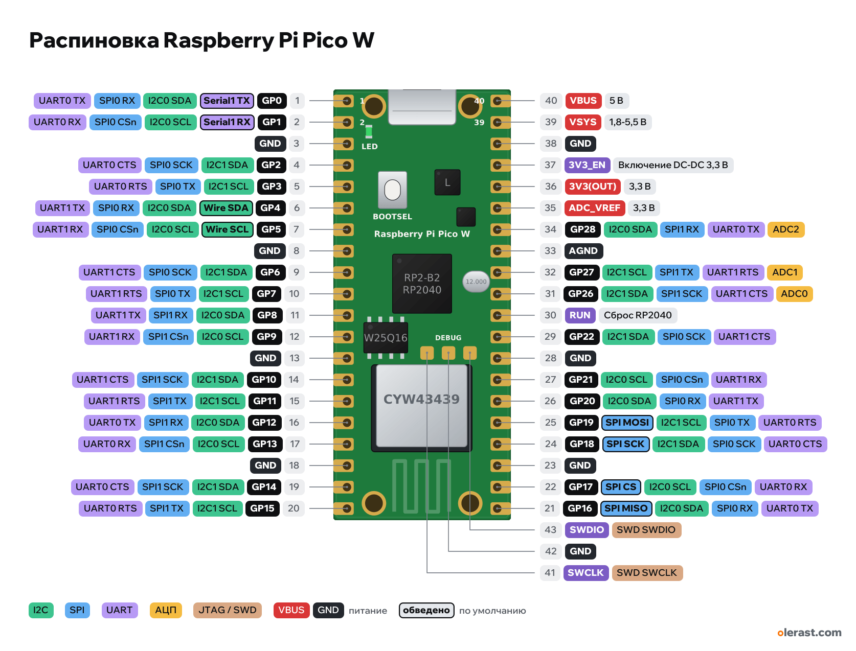
Raspberry Pi Pico W pinout
Raspberry Pi Pico W, RP2040, 3.3 V logic, 21×51 mm, 43 pins
verified15.10.2026
- 1GP0Serial1 TXI2C0 SDASPI0 RXUART0 TX
- 2GP1Serial1 RXI2C0 SCLSPI0 CSnUART0 RX
- 3GND
- 4GP2I2C1 SDASPI0 SCKUART0 CTS
- 5GP3I2C1 SCLSPI0 TXUART0 RTS
- 6GP4Wire SDAI2C0 SDASPI0 RXUART1 TX
- 7GP5Wire SCLI2C0 SCLSPI0 CSnUART1 RX
- 8GND
- 9GP6I2C1 SDASPI0 SCKUART1 CTS
- 10GP7I2C1 SCLSPI0 TXUART1 RTS
- 11GP8I2C0 SDASPI1 RXUART1 TX
- 12GP9I2C0 SCLSPI1 CSnUART1 RX
- 13GND
- 14GP10I2C1 SDASPI1 SCKUART1 CTS
- 15GP11I2C1 SCLSPI1 TXUART1 RTS
- 16GP12I2C0 SDASPI1 RXUART0 TX
- 17GP13I2C0 SCLSPI1 CSnUART0 RX
- 18GND
- 19GP14I2C1 SDASPI1 SCKUART0 CTS
- 20GP15I2C1 SCLSPI1 TXUART0 RTS
- 40VBUS5 V
- 39VSYS1.8-5.5 V
- 38GND
- 373V3_ENDC-DC 3.3 V enable
- 363V3(OUT)3.3 V
- 35ADC_VREF3.3 V
- 34GP28I2C0 SDASPI1 RXUART0 TXADC2
- 33AGND
- 32GP27I2C1 SCLSPI1 TXUART1 RTSADC1
- 31GP26I2C1 SDASPI1 SCKUART1 CTSADC0
- 30RUNRP2040 reset
- 29GP22I2C1 SDASPI0 SCKUART1 CTS
- 28GND
- 27GP21I2C0 SCLSPI0 CSnUART1 RX
- 26GP20I2C0 SDASPI0 RXUART1 TX
- 25GP19SPI MOSII2C1 SCLSPI0 TXUART0 RTS
- 24GP18SPI SCKI2C1 SDASPI0 SCKUART0 CTS
- 23GND
- 22GP17SPI CSI2C0 SCLSPI0 CSnUART0 RX
- 21GP16SPI MISOI2C0 SDASPI0 RXUART0 TX
- 43SWDIOSWD SWDIO
- 42GND
- 41SWCLKSWD SWCLK
Top view, USB at the top.
BuyCompareDownload PNG- Chip
- RP2040, Infineon CYW43439 (Wi-Fi + Bluetooth)
- Logic
- 3.3 V
- Power
- Micro-USB 4.75-5.25 VVSYS 1.8-5.5 VVBUS
- Defaults in arduino-pico
- I2C: SDA 4, SCL 5SPI: MOSI 19, MISO 16, SCK 18, SS 17UART: TX 0, RX 1
Which Raspberry Pi Pico W pins are safe to use
Free to use
GP0-22, GP26-28
Important
- 3.3 V logic, do not apply 5 V to a GPIO.
- The GP0…GP28 labels are printed on the back of the board; the top has only pin numbers 1, 2, 39, 40.
- GP23 is radio power enable (WL_ON), GP24 is radio data/IRQ, GP25 is radio CS, GP29 is radio clock and VSYS/3 measurement (ADC3). The LED is on WL_GPIO0 of the CYW43439 chip, in Arduino and MicroPython it is LED_BUILTIN / "LED".
- ADC: GP26–GP28 (ADC0–ADC2), 12-bit, 0–3.3 V (ADC_VREF).
- The placement of small components in the drawing is approximate (from the datasheet drawing and render); pins and holes follow the drawing dimensions.
- Any GPIO can be PWM, while UART, I2C and SPI are assigned to pins from their own group (function table in the chip datasheet).
- 3V3(OUT) is the output of the built-in DC-DC, not an input.
All pins
| Label | Number | Functions | Limits | Check |
|---|---|---|---|---|
| GP0 | GPIO0, pin 1 | interruptSPI0 RX (MISO)UART0 TXI2C0 SDAPWM 0APIO0, PIO1Serial1 TX | not 5 V tolerant | verified |
| GP1 | GPIO1, pin 2 | interruptSPI0 CSnUART0 RXI2C0 SCLPWM 0BPIO0, PIO1Serial1 RX | not 5 V tolerant | verified |
| GND | pin 3 | Ground | verified | |
| GP2 | GPIO2, pin 4 | interruptSPI0 SCKUART0 CTSI2C1 SDAPWM 1APIO0, PIO1 | not 5 V tolerant | verified |
| GP3 | GPIO3, pin 5 | interruptSPI0 TX (MOSI)UART0 RTSI2C1 SCLPWM 1BPIO0, PIO1 | not 5 V tolerant | verified |
| GP4 | GPIO4, pin 6 | interruptSPI0 RX (MISO)UART1 TXI2C0 SDAPWM 2APIO0, PIO1Wire SDA | not 5 V tolerant | verified |
| GP5 | GPIO5, pin 7 | interruptSPI0 CSnUART1 RXI2C0 SCLPWM 2BPIO0, PIO1Wire SCL | not 5 V tolerant | verified |
| GND | pin 8 | Ground | verified | |
| GP6 | GPIO6, pin 9 | interruptSPI0 SCKUART1 CTSI2C1 SDAPWM 3APIO0, PIO1 | not 5 V tolerant | verified |
| GP7 | GPIO7, pin 10 | interruptSPI0 TX (MOSI)UART1 RTSI2C1 SCLPWM 3BPIO0, PIO1 | not 5 V tolerant | verified |
| GP8 | GPIO8, pin 11 | interruptSPI1 RX (MISO)UART1 TXI2C0 SDAPWM 4APIO0, PIO1 | not 5 V tolerant | verified |
| GP9 | GPIO9, pin 12 | interruptSPI1 CSnUART1 RXI2C0 SCLPWM 4BPIO0, PIO1 | not 5 V tolerant | verified |
| GND | pin 13 | Ground | verified | |
| GP10 | GPIO10, pin 14 | interruptSPI1 SCKUART1 CTSI2C1 SDAPWM 5APIO0, PIO1 | not 5 V tolerant | verified |
| GP11 | GPIO11, pin 15 | interruptSPI1 TX (MOSI)UART1 RTSI2C1 SCLPWM 5BPIO0, PIO1 | not 5 V tolerant | verified |
| GP12 | GPIO12, pin 16 | interruptSPI1 RX (MISO)UART0 TXI2C0 SDAPWM 6APIO0, PIO1 | not 5 V tolerant | verified |
| GP13 | GPIO13, pin 17 | interruptSPI1 CSnUART0 RXI2C0 SCLPWM 6BPIO0, PIO1 | not 5 V tolerant | verified |
| GND | pin 18 | Ground | verified | |
| GP14 | GPIO14, pin 19 | interruptSPI1 SCKUART0 CTSI2C1 SDAPWM 7APIO0, PIO1 | not 5 V tolerant | verified |
| GP15 | GPIO15, pin 20 | interruptSPI1 TX (MOSI)UART0 RTSI2C1 SCLPWM 7BPIO0, PIO1 | not 5 V tolerant | verified |
| VBUS | pin 40 | 5 V | power inputpower output | verified5 V straight from the USB connector. If the board is not powered over USB, this is whatever is applied to the USB host, or nothing. |
| VSYS | pin 39 | 5 V | power inputpower output | verifiedMain power input 1.8–5.5 V for the built-in DC-DC. From USB, VBUS comes here through a Schottky diode. |
| GND | pin 38 | Ground | verified | |
| 3V3_EN | pin 37 | DC-DC 3.3 V enable (low = off) | onboard pull-up | verifiedPulled up to VSYS on the board. Shorting it to ground turns the board off. |
| 3V3(OUT) | pin 36 | 3.3 V | power output | verified3.3 V DC-DC output for sensors. Recommended load up to 300 mA. |
| ADC_VREF | pin 35 | 3.3 V | power inputpower output | verifiedADC reference voltage, 3.3 V through a filter on the board. An external reference can be applied. |
| GP28 | GPIO28, pin 34 | interruptSPI1 RX (MISO)UART0 TXI2C0 SDAPWM 6APIO0, PIO1ADC2 | not 5 V tolerant | verified |
| AGND | pin 33 | Ground | verifiedAnalog ground for the ADC (GP26–GP29). Can be used as regular ground. | |
| GP27 | GPIO27, pin 32 | interruptSPI1 TX (MOSI)UART1 RTSI2C1 SCLPWM 5BPIO0, PIO1ADC1 | not 5 V tolerant | verified |
| GP26 | GPIO26, pin 31 | interruptSPI1 SCKUART1 CTSI2C1 SDAPWM 5APIO0, PIO1ADC0 | not 5 V tolerant | verified |
| RUN | pin 30 | RP2040 reset (low = reset) | verifiedPulled up to the supply inside the chip. A button between RUN and GND is a reset button. | |
| GP22 | GPIO22, pin 29 | interruptSPI0 SCKUART1 CTSI2C1 SDAPWM 3APIO0, PIO1 | not 5 V tolerant | verified |
| GND | pin 28 | Ground | verified | |
| GP21 | GPIO21, pin 27 | interruptSPI0 CSnUART1 RXI2C0 SCLPWM 2BPIO0, PIO1 | not 5 V tolerant | verified |
| GP20 | GPIO20, pin 26 | interruptSPI0 RX (MISO)UART1 TXI2C0 SDAPWM 2APIO0, PIO1 | not 5 V tolerant | verified |
| GP19 | GPIO19, pin 25 | interruptSPI0 TX (MOSI)UART0 RTSI2C1 SCLPWM 1BPIO0, PIO1SPI MOSI | not 5 V tolerant | verified |
| GP18 | GPIO18, pin 24 | interruptSPI0 SCKUART0 CTSI2C1 SDAPWM 1APIO0, PIO1SPI SCK | not 5 V tolerant | verified |
| GND | pin 23 | Ground | verified | |
| GP17 | GPIO17, pin 22 | interruptSPI0 CSnUART0 RXI2C0 SCLPWM 0BPIO0, PIO1SPI CS | not 5 V tolerant | verified |
| GP16 | GPIO16, pin 21 | interruptSPI0 RX (MISO)UART0 TXI2C0 SDAPWM 0APIO0, PIO1SPI MISO | not 5 V tolerant | verified |
| SWCLK | pin 41 | SWD SWCLK | verified | |
| GND | pin 42 | Ground | verified | |
| SWDIO | pin 43 | SWD SWDIO | verified |
Sources
Every pin is verified against the manufacturer's documents.
- Raspberry Pi Pico W Datasheet (Raspberry Pi)datasheet, checked 15.10.2026size 51×21 mm, pitch 2.54, rows 17.78 mm apart, position of pins and debug pads, functions of VBUS/VSYS/3V3_EN/ADC_VREF/RUN, internal board GPIO
- Raspberry Pi Pico W Pinout (Raspberry Pi)manufacturer pinout, checked 15.10.2026pin numbers 1–40, labels GP0–GP28, GND, VBUS, VSYS, 3V3_EN, 3V3(OUT), ADC_VREF, RUN, SWD
- RP2040 Datasheet (Raspberry Pi), section 1.4.3 GPIO Functionsdatasheet, checked 15.10.2026GPIO functions: SPI, UART, I2C, PWM, PIO per the F1–F9 table, ADC0–3 on GPIO26–29, pins are not 5 V tolerant
- arduino-pico (Earle Philhower): variants/rpipico/pins_arduino.hArduino core, checked 15.10.2026defaults: Serial1 TX 0 RX 1, Wire SDA 4 SCL 5, SPI MISO 16 CS 17 SCK 18 MOSI 19
Size: per the datasheet mechanical drawing.
FAQ
- Which Raspberry Pi Pico W pins are I2C, SPI and UART?
- By default in arduino-pico: I2C: SDA GP4, SCL GP5; SPI: MOSI GP19, MISO GP16, SCK GP18, SS GP17; UART: TX GP0, RX GP1.
- Are the Raspberry Pi Pico W pins 5 V tolerant?
- No. The logic is 3.3 V and the pins are not 5 V tolerant: use a divider or a level shifter for 5 V signals.
You might also need
Schematic with this board
schematic builder with the board already placed
Flash this board
upload a sketch or .bin to this board from the browser
Power budget
will the regulator cope and how long the battery lasts
Calculators
LED resistor, voltage divider, battery runtime, 3D print cost, LED strip power supply and pF, nF, µF conversion
Similar boards
Next
Need firmware or a device built on RP2040? I'll build it to order