STM32 Blue Pill (STM32F103C8T6) pinout
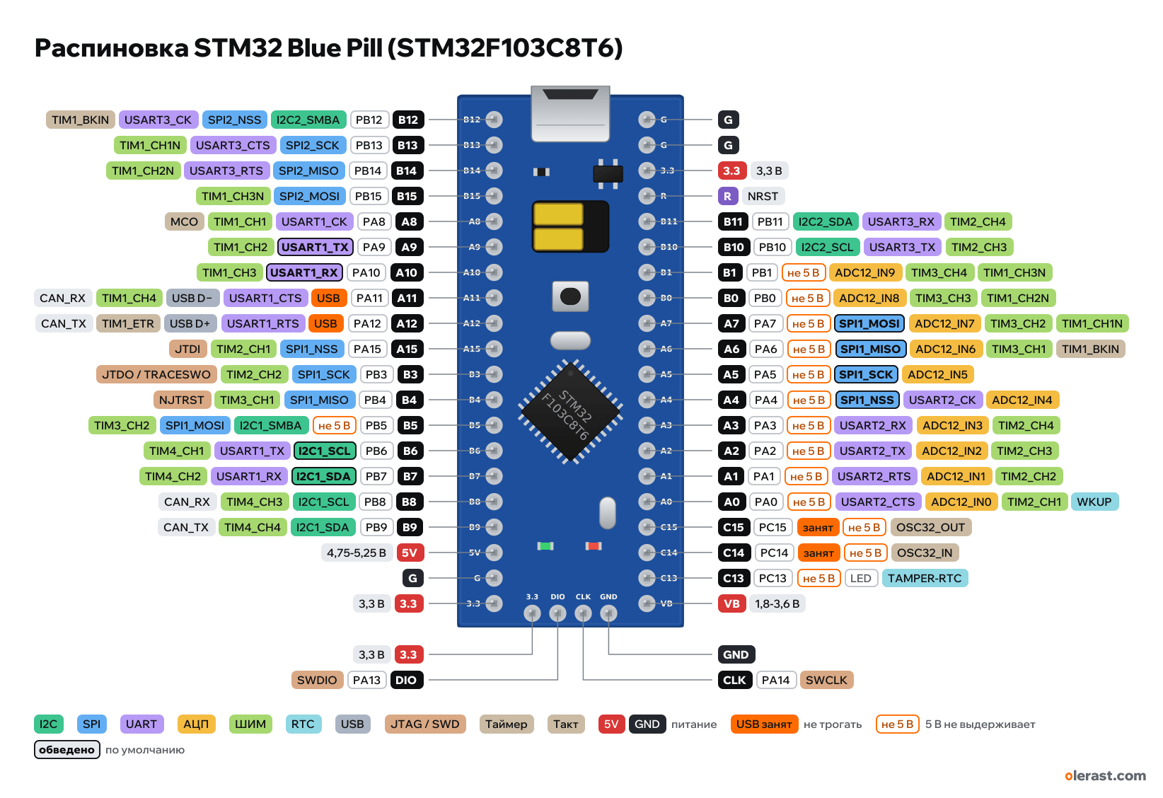
STM32 Blue Pill (STM32F103C8T6), STM32F103C8T6, 3.3 V logic, 22.6×53 mm, 44 pins
partly verified15.10.2026
- B12PB12I2C2_SMBASPI2_NSSUSART3_CKTIM1_BKIN
- B13PB13SPI2_SCKUSART3_CTSPWM TIM1_CH1N
- B14PB14SPI2_MISOUSART3_RTSPWM TIM1_CH2N
- B15PB15SPI2_MOSIPWM TIM1_CH3N
- A8PA8USART1_CKPWM TIM1_CH1MCO
- A9PA9USART1_TXPWM TIM1_CH2
- A10PA10USART1_RXPWM TIM1_CH3
- A11PA11USBUSART1_CTSUSB D−PWM TIM1_CH4CAN_RX
- A12PA12USBUSART1_RTSUSB D+TIM1_ETRCAN_TX
- A15PA15SPI1_NSSPWM TIM2_CH1JTDI
- B3PB3SPI1_SCKPWM TIM2_CH2JTDO / TRACESWO
- B4PB4SPI1_MISOPWM TIM3_CH1NJTRST
- B5PB5not 5 VI2C1_SMBASPI1_MOSIPWM TIM3_CH2
- B6PB6I2C1_SCLUSART1_TXPWM TIM4_CH1
- B7PB7I2C1_SDAUSART1_RXPWM TIM4_CH2
- B8PB8I2C1_SCLPWM TIM4_CH3CAN_RX
- B9PB9I2C1_SDAPWM TIM4_CH4CAN_TX
- 5V4.75-5.25 V
- G
- 3.33.3 V
- 3.33.3 V
- DIOPA13SWDIO
- G
- G
- 3.33.3 V
- RNRST
- B11PB11I2C2_SDAUSART3_RXPWM TIM2_CH4
- B10PB10I2C2_SCLUSART3_TXPWM TIM2_CH3
- B1PB1not 5 VADC12_IN9PWM TIM3_CH4PWM TIM1_CH3N
- B0PB0not 5 VADC12_IN8PWM TIM3_CH3PWM TIM1_CH2N
- A7PA7not 5 VSPI1_MOSIADC12_IN7PWM TIM3_CH2PWM TIM1_CH1N
- A6PA6not 5 VSPI1_MISOADC12_IN6PWM TIM3_CH1TIM1_BKIN
- A5PA5not 5 VSPI1_SCKADC12_IN5
- A4PA4not 5 VSPI1_NSSUSART2_CKADC12_IN4
- A3PA3not 5 VUSART2_RXADC12_IN3PWM TIM2_CH4
- A2PA2not 5 VUSART2_TXADC12_IN2PWM TIM2_CH3
- A1PA1not 5 VUSART2_RTSADC12_IN1PWM TIM2_CH2
- A0PA0not 5 VUSART2_CTSADC12_IN0PWM TIM2_CH1WKUP
- C15PC15busynot 5 VOSC32_OUT
- C14PC14busynot 5 VOSC32_IN
- C13PC13not 5 VLEDTAMPER-RTC
- VB1.8-3.6 V
- GND
- CLKPA14SWCLK
Top view, USB at the top, SWD at the bottom.
CompareDownload PNG- Chip
- STM32F103C8T6
- Logic
- 3.3 V
- Power
- Micro-USB 4.75-5.25 V5V 4.75-5.25 V3.3 3-3.6 VVB 1.8-3.6 V
Which STM32 Blue Pill (STM32F103C8T6) pins are safe to use
Free to use
PA0-PA10, PA13-PA15, PB0, PB1, PB3-PB15
Use with care
- PA11, PA12: USB lines: use them and you lose USB flashing and the serial port.
- PC13: onboard LED.
Leave alone
- PC14, PC15: internal board lines.
Important
- 3.3 V logic. Only FT pins tolerate 5 V: PA8–PA15, PB2–PB4, PB6–PB15 (and only when the board is powered). Not tolerant: PA0–PA7, PB0, PB1, PB5, PC13–PC15.
- USB may not enumerate: the D+ pull-up (R10 on PA12) is 10 or 4.7 kΩ on most boards instead of 1.5 kΩ. Replacing R10 with 1.5 kΩ fixes it.
- No USB bootloader from the factory: first flash via ST-Link (SWD at the bottom) or via USART1 (PA9, PA10) with BOOT0 = 1. For USB flashing, install a bootloader (STM32duino-bootloader, HID).
- 5V is tied directly to VBUS: do not apply external 5 V while USB is plugged in.
- PC13–PC15 are weak: sink current up to 3 mA, up to 2 MHz, no current sourcing. PC14/PC15 carry the 32.768 kHz crystal.
- PA15, PB3, PB4 are taken by JTAG after reset; stm32duino disables JTAG itself (SWD stays).
- The chip is often not original: CS32F103, CKS32F103 (IDCODE 0x2BA01477, in OpenOCD set CPUTAPID 0x2ba01477), GD32, APM32. STM32CubeIDE and ST-Link may refuse to work with clones.
- Small components, the BOOT header and the SWD connector are drawn approximately; pin rows follow the KiCad footprint.
- 3.3 V regulator, 300 mA (RT9193 per the schematic, often TX6211B or another on real boards).
Revisions and clones
- Flash: the C8 guarantees 64 KB, most chips physically have 128 KB (not guaranteed by ST). Some boards carry the STM32F103CBT6 (128 KB).
- Clones differ in regulator, R10 value (10 or 4.7 kΩ, rarely 1.5), LED colors, and sometimes the SWD connector is not soldered.
- The STM32F103 "Black Pill" (RobotDyn) is a different board with a different pinout; the WeAct Black Pill uses an STM32F401/F411.
All pins
| Label | Number | Functions | Limits | Check |
|---|---|---|---|---|
| B12 | PB12 | SPI2_NSSI2C2_SMBAUSART3_CKTIM1_BKINEXTI12 | 5 V tolerant | verified5 V tolerant input (FT) when the board is powered with 3.3 V. Output is still 3.3 V. Do not apply 5 V in analog mode. |
| B13 | PB13 | SPI2_SCKPWM TIM1_CH1NUSART3_CTSEXTI13 | 5 V tolerant | verified5 V tolerant input (FT) when the board is powered with 3.3 V. Output is still 3.3 V. Do not apply 5 V in analog mode. |
| B14 | PB14 | SPI2_MISOPWM TIM1_CH2NUSART3_RTSEXTI14 | 5 V tolerant | verified5 V tolerant input (FT) when the board is powered with 3.3 V. Output is still 3.3 V. Do not apply 5 V in analog mode. |
| B15 | PB15 | SPI2_MOSIPWM TIM1_CH3NEXTI15 | 5 V tolerant | verified5 V tolerant input (FT) when the board is powered with 3.3 V. Output is still 3.3 V. Do not apply 5 V in analog mode. |
| A8 | PA8 | PWM TIM1_CH1USART1_CKMCO (clock output)EXTI8 | 5 V tolerant | verified5 V tolerant input (FT) when the board is powered with 3.3 V. Output is still 3.3 V. Do not apply 5 V in analog mode. |
| A9 | PA9 | USART1_TX (Serial)PWM TIM1_CH2EXTI9 | 5 V tolerant | verified5 V tolerant input (FT) when the board is powered with 3.3 V. Output is still 3.3 V. Do not apply 5 V in analog mode. |
| A10 | PA10 | USART1_RX (Serial)PWM TIM1_CH3EXTI10 | 5 V tolerant | verifiedThe built-in ST bootloader (BOOT0 = 1) listens on USART1: PA9 TX, PA10 RX.5 V tolerant input (FT) when the board is powered with 3.3 V. Output is still 3.3 V. Do not apply 5 V in analog mode. |
| A11 | PA11 | USB D− (USBDM)CAN_RXPWM TIM1_CH4USART1_CTSEXTI11 | USB line5 V tolerant | verifiedCAN and USB do not work at the same time on the F103 (shared memory).5 V tolerant input (FT) when the board is powered with 3.3 V. Output is still 3.3 V. Do not apply 5 V in analog mode.USB D− line (through 20 Ω): leave it free while USB is in use. |
| A12 | PA12 | USB D+ (USBDP)CAN_TXTIM1_ETRUSART1_RTSEXTI12 | USB line5 V tolerantonboard pull-up | verifiedCAN and USB do not work at the same time on the F103 (shared memory).5 V tolerant input (FT) when the board is powered with 3.3 V. Output is still 3.3 V. Do not apply 5 V in analog mode.USB D+ line (through 20 Ω), pull-up R10 to 3.3 V. On most boards R10 is 10 or 4.7 kΩ instead of the 1.5 kΩ in the USB spec, so some computers do not detect the board. Fix: replace R10 with 1.5 kΩ, or add a 1.8 kΩ resistor from PA12 to 3.3 V. |
| A15 | PA15 | JTDIPWM TIM2_CH1 (remap)SPI1_NSS (remap)EXTI15 | 5 V tolerant | verifiedAfter reset this pin is JTAG. It works as a normal GPIO once JTAG is disabled (SWD stays); stm32duino does this itself on pinMode.5 V tolerant input (FT) when the board is powered with 3.3 V. Output is still 3.3 V. Do not apply 5 V in analog mode. |
| B3 | PB3 | JTDO / TRACESWOPWM TIM2_CH2 (remap)SPI1_SCK (remap)EXTI3 | 5 V tolerant | verifiedAfter reset this pin is JTAG. It works as a normal GPIO once JTAG is disabled (SWD stays); stm32duino does this itself on pinMode.5 V tolerant input (FT) when the board is powered with 3.3 V. Output is still 3.3 V. Do not apply 5 V in analog mode. |
| B4 | PB4 | NJTRSTPWM TIM3_CH1 (remap)SPI1_MISO (remap)EXTI4 | 5 V tolerant | verifiedAfter reset this pin is JTAG. It works as a normal GPIO once JTAG is disabled (SWD stays); stm32duino does this itself on pinMode.5 V tolerant input (FT) when the board is powered with 3.3 V. Output is still 3.3 V. Do not apply 5 V in analog mode. |
| B5 | PB5 | I2C1_SMBAPWM TIM3_CH2 (remap)SPI1_MOSI (remap)EXTI5 | not 5 V tolerant | verifiedThe only pin among PB2–PB15 that is not FT: do not apply 5 V.Not 5 V tolerant (not an FT pin): input must not exceed VDD + 0.3 V. |
| B6 | PB6 | I2C1_SCL (Wire)PWM TIM4_CH1USART1_TX (remap)EXTI6 | 5 V tolerant | verified5 V tolerant input (FT) when the board is powered with 3.3 V. Output is still 3.3 V. Do not apply 5 V in analog mode. |
| B7 | PB7 | I2C1_SDA (Wire)PWM TIM4_CH2USART1_RX (remap)EXTI7 | 5 V tolerant | verified5 V tolerant input (FT) when the board is powered with 3.3 V. Output is still 3.3 V. Do not apply 5 V in analog mode. |
| B8 | PB8 | PWM TIM4_CH3I2C1_SCL (remap)CAN_RX (remap)EXTI8 | 5 V tolerant | verified5 V tolerant input (FT) when the board is powered with 3.3 V. Output is still 3.3 V. Do not apply 5 V in analog mode. |
| B9 | PB9 | PWM TIM4_CH4I2C1_SDA (remap)CAN_TX (remap)EXTI9 | 5 V tolerant | verified5 V tolerant input (FT) when the board is powered with 3.3 V. Output is still 3.3 V. Do not apply 5 V in analog mode. |
| 5V | 5 V | power inputpower output | verifiedConnected directly to micro-USB VBUS, no diode: external 5 V with USB plugged in will flow back into the computer. | |
| G | Ground | verifiedLabelled on other revisions as: GND | ||
| 3.3 | 3.3 V | power inputpower output | verifiedLabelled on other revisions as: 3V3 | |
| G | Ground | verifiedLabelled on other revisions as: GND | ||
| G | Ground | verifiedLabelled on other revisions as: GND | ||
| 3.3 | 3.3 V | power inputpower output | verifiedLabelled on other revisions as: 3V3 | |
| R | NRST: reset (low = reset) | verifiedLabelled on other revisions as: RST, NRST | ||
| B11 | PB11 | I2C2_SDAUSART3_RX (Serial3)PWM TIM2_CH4 (remap)EXTI11 | 5 V tolerant | verified5 V tolerant input (FT) when the board is powered with 3.3 V. Output is still 3.3 V. Do not apply 5 V in analog mode. |
| B10 | PB10 | I2C2_SCLUSART3_TX (Serial3)PWM TIM2_CH3 (remap)EXTI10 | 5 V tolerant | verified5 V tolerant input (FT) when the board is powered with 3.3 V. Output is still 3.3 V. Do not apply 5 V in analog mode. |
| B1 | PB1 | ADC12_IN9PWM TIM3_CH4PWM TIM1_CH3N (remap)EXTI1 | not 5 V tolerant | verifiedNot 5 V tolerant (not an FT pin): input must not exceed VDD + 0.3 V. |
| B0 | PB0 | ADC12_IN8PWM TIM3_CH3PWM TIM1_CH2N (remap)EXTI0 | not 5 V tolerant | verifiedNot 5 V tolerant (not an FT pin): input must not exceed VDD + 0.3 V. |
| A7 | PA7 | ADC12_IN7SPI1_MOSIPWM TIM3_CH2PWM TIM1_CH1N (remap)EXTI7 | not 5 V tolerant | verifiedNot 5 V tolerant (not an FT pin): input must not exceed VDD + 0.3 V. |
| A6 | PA6 | ADC12_IN6SPI1_MISOPWM TIM3_CH1TIM1_BKIN (remap)EXTI6 | not 5 V tolerant | verifiedNot 5 V tolerant (not an FT pin): input must not exceed VDD + 0.3 V. |
| A5 | PA5 | ADC12_IN5SPI1_SCKEXTI5 | not 5 V tolerant | verifiedNot 5 V tolerant (not an FT pin): input must not exceed VDD + 0.3 V. |
| A4 | PA4 | ADC12_IN4SPI1_NSS (SS)USART2_CKEXTI4 | not 5 V tolerant | verifiedNot 5 V tolerant (not an FT pin): input must not exceed VDD + 0.3 V. |
| A3 | PA3 | ADC12_IN3PWM TIM2_CH4USART2_RX (Serial2)EXTI3 | not 5 V tolerant | verifiedNot 5 V tolerant (not an FT pin): input must not exceed VDD + 0.3 V. |
| A2 | PA2 | ADC12_IN2PWM TIM2_CH3USART2_TX (Serial2)EXTI2 | not 5 V tolerant | verifiedNot 5 V tolerant (not an FT pin): input must not exceed VDD + 0.3 V. |
| A1 | PA1 | ADC12_IN1PWM TIM2_CH2USART2_RTSEXTI1 | not 5 V tolerant | verifiedNot 5 V tolerant (not an FT pin): input must not exceed VDD + 0.3 V. |
| A0 | PA0 | ADC12_IN0PWM TIM2_CH1USART2_CTSWKUP (wake from Standby)EXTI0 | not 5 V tolerant | verifiedNot 5 V tolerant (not an FT pin): input must not exceed VDD + 0.3 V. |
| C15 | PC15 | OSC32_OUT (32.768 kHz crystal)EXTI15 | not 5 V tolerantused inside the board | verifiedWeak pin (PC13–PC15): sink current up to 3 mA, frequency up to 2 MHz, cannot source current, only one of the three may switch at a time, load up to 30 pF (DS5319, pin table note).Not 5 V tolerant (not an FT pin): input must not exceed VDD + 0.3 V.The board has a 32.768 kHz crystal: unreliable as a GPIO. |
| C14 | PC14 | OSC32_IN (32.768 kHz crystal)EXTI14 | not 5 V tolerantused inside the board | verifiedWeak pin (PC13–PC15): sink current up to 3 mA, frequency up to 2 MHz, cannot source current, only one of the three may switch at a time, load up to 30 pF (DS5319, pin table note).Not 5 V tolerant (not an FT pin): input must not exceed VDD + 0.3 V.The board has a 32.768 kHz crystal: unreliable as a GPIO. |
| C13 | PC13 | TAMPER-RTCEXTI13 | not 5 V tolerantonboard LED | verifiedWeak pin (PC13–PC15): sink current up to 3 mA, frequency up to 2 MHz, cannot source current, only one of the three may switch at a time, load up to 30 pF (DS5319, pin table note).Not 5 V tolerant (not an FT pin): input must not exceed VDD + 0.3 V.LED through 510 Ω to 3.3 V: lights when LOW. LED_BUILTIN. |
| VB | 3.3 V | power input | verifiedSupply for the clock and backup registers.Labelled on other revisions as: VBAT | |
| 3.3 | 3.3 V | power inputpower output | not from manufacturerSWD order (3.3, DIO, CLK, GND) per stm32-base; the connector position at the end is drawn approximately (no drawing available). Check the silkscreen on the board.Labelled on other revisions as: 3V3 | |
| DIO | PA13 | SWDIO (JTMS)EXTI13 | 5 V tolerant | not from manufacturerSWD order (3.3, DIO, CLK, GND) per stm32-base; the connector position at the end is drawn approximately (no drawing available). Check the silkscreen on the board.SWD line: if you use it as a GPIO, ST-Link connects only with "connect under reset".5 V tolerant input (FT) when the board is powered with 3.3 V. Output is still 3.3 V. Do not apply 5 V in analog mode.Labelled on other revisions as: SWDIO, IO |
| CLK | PA14 | SWCLK (JTCK)EXTI14 | 5 V tolerant | not from manufacturerSWD order (3.3, DIO, CLK, GND) per stm32-base; the connector position at the end is drawn approximately (no drawing available). Check the silkscreen on the board.SWD line: if you use it as a GPIO, ST-Link connects only with "connect under reset".5 V tolerant input (FT) when the board is powered with 3.3 V. Output is still 3.3 V. Do not apply 5 V in analog mode.Labelled on other revisions as: SWCLK, DCLK |
| GND | Ground | not from manufacturerSWD order (3.3, DIO, CLK, GND) per stm32-base; the connector position at the end is drawn approximately (no drawing available). Check the silkscreen on the board. |
Sources
Not verified against the manufacturer: 4 of 44 pins. The pin card says what confirms each one and where sources disagree.
- Blue Pill schematic (VCC-GND, 2016), copy from stm32-base.orgschematic, checked 15.10.2026header nets, R10 4.7 kΩ on PA12, 20 Ω on D+ and D−, RT9193-33, BOOT 3×2 header through 100 kΩ, LED PC13 and PWR through 510 Ω from 3.3 V, 8 MHz and 32.768 kHz crystals, 5V = VBUS
- stm32-base.org: STM32F103C8T6 Blue Pillthird-party source, checked 15.10.2026order of both rows and SWD (3.3, DIO, CLK, GND), size 23×53 mm, TX6211B 300 mA regulator on real boards, LED PC13 "Sink", 5V unprotected, D+ pull-up 10 or 4.7 kΩ
- KiCad: YAAJ_BluePill_1.kicad_mod (yet-another-average-joe, copy in the Cantor project)third-party source, checked 15.10.2026outline 22.6×53.0 mm, first pin 3.68 mm from the long edge and 2.37 mm from the USB edge, rows 15.24 mm apart, USB position
- deskthority wiki: Blue Pillthird-party source, checked 15.10.2026wrong R10 value, LED PC13 active low, 5V tied to VBUS, fragile micro-USB
- Greaseweazle wiki: STM32 Fakesthird-party source, checked 15.10.2026STM32F103 clones and fakes (CS32F103, CKS32, GD32, APM32), and how they differ
- EEVblog forum: unexpected IDCODE flashing bluepill clonethird-party source, checked 15.10.2026CS32/CKS32 have SW-DP IDCODE 0x2BA01477 instead of 0x1BA01477, OpenOCD needs set CPUTAPID
- STM32F103x8/xB Datasheet (ST DS5319, DocID 13587), Table 5 Medium-density pin definitions (checked against Rev 14)datasheet, checked 15.10.2026PB5 is not FT; also not FT: PA0–PA7, PB0, PB1, PC13–PC15; default and remap functions of LQFP48 pins, pin type FT (5 V tolerant) or not, PC13–PC15 limits, ADC12_IN0–9 on PA0–PA7, PB0, PB1
- stm32duino: variants/STM32F1xx/F103C8T_F103CB(T-U)/variant_PILL_F103Cx.hArduino core, checked 15.10.2026defaults: LED_BUILTIN PC13 (LED_GREEN), Serial USART1 PA9/PA10, Wire PB7 SDA / PB6 SCL, SPI PA7 MOSI / PA6 MISO / PA5 SCK / PA4 SS
- ST STM32_open_pin_data: STM32F103C(8-B)Tx.xmldatasheet, checked 15.10.2026LQFP48 pin numbers and the signal of each pin (checked against the datasheet table)
Size: 22.6×53.0 mm per the KiCad footprint (stm32-base says 23×53); clones differ by tenths of a mm (approximate).
FAQ
- Which pin is the STM32 Blue Pill (STM32F103C8T6) LED on?
- LED on PC13 (lights on LOW).
- Are the STM32 Blue Pill (STM32F103C8T6) pins 5 V tolerant?
- Only these pins tolerate 5 V: PA8-PA15, PB3, PB4, PB6-PB15. The rest are 3.3 V, so feed them a 5 V signal through a divider or a level shifter.
You might also need
Schematic with this board
schematic builder with the board already placed
Flash this board
upload a sketch or .bin to this board from the browser
Power budget
will the regulator cope and how long the battery lasts
Calculators
LED resistor, voltage divider, battery runtime, 3D print cost, LED strip power supply and pF, nF, µF conversion
Similar boards
Next
Need firmware or a device built on STM32? I'll build it to order