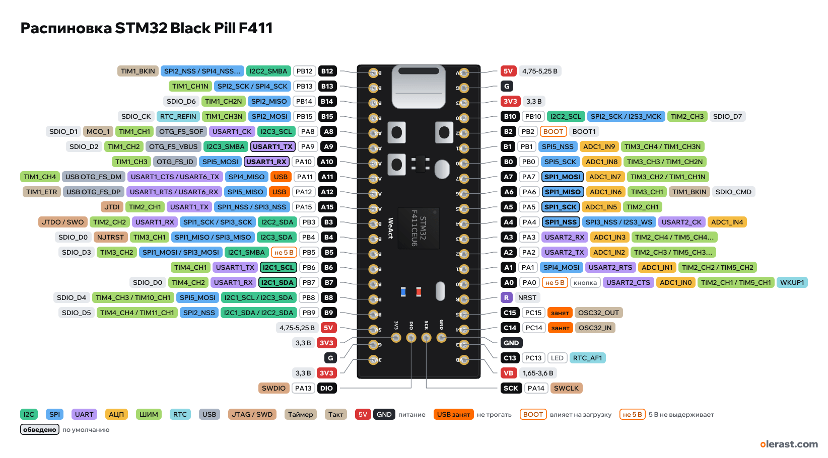
STM32 Black Pill F411 pinout
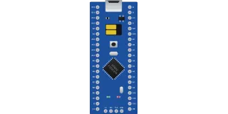
WeAct Black Pill STM32F411CEU6 (V3.1, USB-C), STM32F411CEU6, 3.3 V logic, 52.81×20.78 mm, 44 pins
- B12PB12I2C2_SMBASPI2_NSS / SPI4_NSS…TIM1_BKIN
- B13PB13SPI2_SCK / SPI4_SCKPWM TIM1_CH1N
- B14PB14SPI2_MISOPWM TIM1_CH2NSDIO_D6
- B15PB15SPI2_MOSIPWM TIM1_CH3NRTC_REFINSDIO_CK
- A8PA8I2C3_SCLUSART1_CKOTG_FS_SOFPWM TIM1_CH1MCO_1SDIO_D1
- A9PA9USART1_TXI2C3_SMBAOTG_FS_VBUSPWM TIM1_CH2SDIO_D2
- A10PA10USART1_RXSPI5_MOSIOTG_FS_IDPWM TIM1_CH3
- A11PA11USBSPI4_MISOUSART1_CTS / USART6_TXUSB OTG_FS_DMPWM TIM1_CH4
- A12PA12USBSPI5_MISOUSART1_RTS / USART6_RXUSB OTG_FS_DPTIM1_ETR
- A15PA15SPI1_NSS / SPI3_NSSUSART1_TXPWM TIM2_CH1JTDI
- B3PB3I2C2_SDASPI1_SCK / SPI3_SCKUSART1_RXPWM TIM2_CH2JTDO / SWO
- B4PB4I2C3_SDASPI1_MISO / SPI3_MISOPWM TIM3_CH1NJTRSTSDIO_D0
- B5PB5not 5 VI2C1_SMBASPI1_MOSI / SPI3_MOSIPWM TIM3_CH2SDIO_D3
- B6PB6I2C1_SCLUSART1_TXPWM TIM4_CH1
- B7PB7I2C1_SDAUSART1_RXPWM TIM4_CH2SDIO_D0
- B8PB8I2C1_SCL / I2C3_SDASPI5_MOSIPWM TIM4_CH3 /…SDIO_D4
- B9PB9I2C1_SDA / I2C2_SDASPI2_NSSPWM TIM4_CH4 /…SDIO_D5
- 5V4.75-5.25 V
- 3V33.3 V
- G
- 3V33.3 V
- DIOPA13SWDIO
- 5V4.75-5.25 V
- G
- 3V33.3 V
- B10PB10I2C2_SCLSPI2_SCK / I2S3_MCKPWM TIM2_CH3SDIO_D7
- B2PB2BOOTBOOT1
- B1PB1SPI5_NSSADC1_IN9PWM TIM3_CH4 /…
- B0PB0SPI5_SCKADC1_IN8PWM TIM3_CH3 /…
- A7PA7SPI1_MOSIADC1_IN7PWM TIM3_CH2 /…
- A6PA6SPI1_MISOADC1_IN6PWM TIM3_CH1TIM1_BKINSDIO_CMD
- A5PA5SPI1_SCKADC1_IN5PWM TIM2_CH1
- A4PA4SPI1_NSSSPI3_NSS / I2S3_WSUSART2_CKADC1_IN4
- A3PA3USART2_RXADC1_IN3PWM TIM2_CH4 /…
- A2PA2USART2_TXADC1_IN2PWM TIM2_CH3 /…
- A1PA1SPI4_MOSIUSART2_RTSADC1_IN1PWM TIM2_CH2 /…
- A0PA0not 5 VbuttonUSART2_CTSADC1_IN0PWM TIM2_CH1 /…WKUP1
- RNRST
- C15PC15busyOSC32_OUT
- C14PC14busyOSC32_IN
- GND
- C13PC13LEDRTC_AF1
- VB1.65-3.6 V
- SCKPA14SWCLK
Top view, USB-C on the left, SWD on the right, rotated 90° on the diagram.
CompareDownload PNG- Chip
- STM32F411CEU6
- Logic
- 3.3 V
- Power
- USB-C 4.75-5.25 V5V 4.75-5.25 V3V3 3-3.6 VVB 1.65-3.6 V
Which STM32 Black Pill F411 pins are safe to use
Free to use
PA1-PA10, PA13-PA15, PB0, PB1, PB3-PB10, PB12-PB15
Use with care
- PA0: onboard button.
- PA11, PA12: USB lines: use them and you lose USB flashing and the serial port.
- PB2: strapping: the level at power-up selects the boot mode.
- PC13: onboard LED.
Leave alone
- PC14, PC15: internal board lines.
Important
- 3.3 V logic. All broken-out GPIO tolerate 5 V except PA0 and PB5 (TC type), and only while 3.3 V power is applied. Don't apply 5 V in ADC mode.
- Flashing without a programmer: hold BOOT0, press and release NRST, release BOOT0 after half a second: the board shows up as DFU (STM32CubeProgrammer, dfu-util). If DFU is not detected, WeAct advises heating or cooling the chip; a floating PA10 also interferes.
- The LED on PC13 lights when LOW. The KEY button on PA0 has no external pull-up: enable INPUT_PULLUP.
- There is no PB11 in the UFQFPN48 package: B12 follows right after B10.
- SWD (DIO = PA13, SCK = PA14) is broken out on a separate header on the right.
- Small components (buttons, crystals, LEDs, regulator) are drawn approximately; pins follow the WeAct V3.1 drawing.
- 3.3 V regulator in a SOT-23 package (AP7343 on V3.0, 300 mA); WeAct doesn't state the type on V3.1. Keep the external load on 3V3 within 100–200 mA.
Revisions and clones
- Black Pill F401CC/F401CE: same board and pinout, weaker chip (84 MHz, 256/512 KB). WeAct discontinued them, sellers sometimes pass F401 off as F411: check the marking.
- Clones without the WeAct logo often copy the old V1.2 schematic (different flash routing) or fit an 8 MHz crystal instead of 25 (stm32duino has the BLACKPILL_F411CE_8M variant).
- Before V3.1: V3.0 with the AP7343 regulator (DFN), V2.0 with flash MISO on PB4, on V2.x 5V is connected to VBUS directly.
All pins
| Label | Number | Functions | Limits | Check |
|---|---|---|---|---|
| 5V | 5 V | power inputpower output | verified | |
| G | Ground | verifiedLabelled on other revisions as: GND | ||
| 3V3 | 3.3 V | power inputpower output | verified | |
| B10 | PB10 | I2C2_SCLPWM TIM2_CH3SPI2_SCK / I2S3_MCKSDIO_D7EXTI10 | 5 V tolerant | verified5 V tolerant as an input (FT) only while 3.3 V power is applied and not in analog mode. The output is still 3.3 V. |
| B2 | PB2 | BOOT1EXTI2 | affects boot (strapping)5 V tolerant | verifiedBOOT1: read at reset together with BOOT0.5 V tolerant as an input (FT) only while 3.3 V power is applied and not in analog mode. The output is still 3.3 V.On the board through 10 kΩ (BOOT1). |
| B1 | PB1 | ADC1_IN9PWM TIM3_CH4 / TIM1_CH3NSPI5_NSSEXTI1 | 5 V tolerant | verified5 V tolerant as an input (FT) only while 3.3 V power is applied and not in analog mode. The output is still 3.3 V. |
| B0 | PB0 | ADC1_IN8PWM TIM3_CH3 / TIM1_CH2NSPI5_SCKEXTI0 | 5 V tolerant | verified5 V tolerant as an input (FT) only while 3.3 V power is applied and not in analog mode. The output is still 3.3 V. |
| A7 | PA7 | ADC1_IN7SPI1_MOSIPWM TIM3_CH2 / TIM1_CH1NEXTI7 | 5 V tolerant | verified5 V tolerant as an input (FT) only while 3.3 V power is applied and not in analog mode. The output is still 3.3 V.Footprint for SPI flash (U3, MOSI) on the back; usually not populated. |
| A6 | PA6 | ADC1_IN6SPI1_MISOPWM TIM3_CH1TIM1_BKINSDIO_CMDEXTI6 | 5 V tolerant | verified5 V tolerant as an input (FT) only while 3.3 V power is applied and not in analog mode. The output is still 3.3 V.Footprint for SPI flash (U3, MISO). |
| A5 | PA5 | ADC1_IN5SPI1_SCKPWM TIM2_CH1EXTI5 | 5 V tolerant | verified5 V tolerant as an input (FT) only while 3.3 V power is applied and not in analog mode. The output is still 3.3 V.Footprint for SPI flash (U3, SCK). |
| A4 | PA4 | ADC1_IN4SPI1_NSS (SS)SPI3_NSS / I2S3_WSUSART2_CKEXTI4 | 5 V tolerant | verified5 V tolerant as an input (FT) only while 3.3 V power is applied and not in analog mode. The output is still 3.3 V.Footprint for SPI flash (U3, CS). |
| A3 | PA3 | ADC1_IN3PWM TIM2_CH4 / TIM5_CH4 / TIM9_CH2USART2_RX (Serial2)EXTI3 | 5 V tolerant | verified5 V tolerant as an input (FT) only while 3.3 V power is applied and not in analog mode. The output is still 3.3 V. |
| A2 | PA2 | ADC1_IN2PWM TIM2_CH3 / TIM5_CH3 / TIM9_CH1USART2_TX (Serial2)EXTI2 | 5 V tolerant | verified5 V tolerant as an input (FT) only while 3.3 V power is applied and not in analog mode. The output is still 3.3 V. |
| A1 | PA1 | ADC1_IN1PWM TIM2_CH2 / TIM5_CH2USART2_RTSSPI4_MOSIEXTI1 | 5 V tolerant | verified5 V tolerant as an input (FT) only while 3.3 V power is applied and not in analog mode. The output is still 3.3 V. |
| A0 | PA0 | ADC1_IN0PWM TIM2_CH1 / TIM5_CH1USART2_CTSWKUP1 (wake from Standby)EXTI0 | not 5 V tolerantonboard button | verifiedNot 5 V tolerant (TC type): at most VDD + 0.3 V on the input.KEY button through 330 Ω to ground, no external pull-up (R4 not populated): pinMode(PA0, INPUT_PULLUP). USER_BTN in stm32duino. |
| R | NRST: reset (low = reset) | verifiedLabelled on other revisions as: NRST | ||
| C15 | PC15 | OSC32_OUT (32.768 kHz crystal)EXTI15 | 5 V tolerantused inside the board | verifiedWeak pin (PC13–PC15): sink current at most 3 mA, frequency up to 2 MHz, cannot source current, switch only one of the three at a time, load capacitance up to 30 pF (DS10314, pin table note).5 V tolerant as an input (FT) only while 3.3 V power is applied and not in analog mode. The output is still 3.3 V.The board has a 32.768 kHz crystal: unreliable as a GPIO. |
| C14 | PC14 | OSC32_IN (32.768 kHz crystal)EXTI14 | 5 V tolerantused inside the board | verifiedWeak pin (PC13–PC15): sink current at most 3 mA, frequency up to 2 MHz, cannot source current, switch only one of the three at a time, load capacitance up to 30 pF (DS10314, pin table note).5 V tolerant as an input (FT) only while 3.3 V power is applied and not in analog mode. The output is still 3.3 V.The board has a 32.768 kHz crystal: unreliable as a GPIO. |
| C13 | PC13 | RTC_AF1 (TAMP / OUT / TS)EXTI13 | 5 V tolerantonboard LED | verifiedWeak pin (PC13–PC15): sink current at most 3 mA, frequency up to 2 MHz, cannot source current, switch only one of the three at a time, load capacitance up to 30 pF (DS10314, pin table note).5 V tolerant as an input (FT) only while 3.3 V power is applied and not in analog mode. The output is still 3.3 V.Blue LED to 3.3 V: lights when LOW. LED_BUILTIN. |
| VB | 3.3 V | power input | verifiedPower for the clock and backup registers. The board has BAT54C diode isolation from 3.3 V.Labelled on other revisions as: VBAT | |
| B12 | PB12 | SPI2_NSS / SPI4_NSS / SPI3_SCKTIM1_BKINI2C2_SMBAEXTI12 | 5 V tolerant | verified5 V tolerant as an input (FT) only while 3.3 V power is applied and not in analog mode. The output is still 3.3 V. |
| B13 | PB13 | SPI2_SCK / SPI4_SCKPWM TIM1_CH1NEXTI13 | 5 V tolerant | verified5 V tolerant as an input (FT) only while 3.3 V power is applied and not in analog mode. The output is still 3.3 V. |
| B14 | PB14 | SPI2_MISOPWM TIM1_CH2NSDIO_D6EXTI14 | 5 V tolerant | verified5 V tolerant as an input (FT) only while 3.3 V power is applied and not in analog mode. The output is still 3.3 V. |
| B15 | PB15 | SPI2_MOSIPWM TIM1_CH3NSDIO_CKRTC_REFINEXTI15 | 5 V tolerant | verified5 V tolerant as an input (FT) only while 3.3 V power is applied and not in analog mode. The output is still 3.3 V. |
| A8 | PA8 | PWM TIM1_CH1I2C3_SCLUSART1_CKOTG_FS_SOFMCO_1SDIO_D1EXTI8 | 5 V tolerant | verified5 V tolerant as an input (FT) only while 3.3 V power is applied and not in analog mode. The output is still 3.3 V. |
| A9 | PA9 | USART1_TX (Serial)PWM TIM1_CH2I2C3_SMBAOTG_FS_VBUSSDIO_D2EXTI9 | 5 V tolerant | verified5 V tolerant as an input (FT) only while 3.3 V power is applied and not in analog mode. The output is still 3.3 V. |
| A10 | PA10 | USART1_RX (Serial)PWM TIM1_CH3SPI5_MOSIOTG_FS_IDEXTI10 | 5 V tolerant | verifiedThe built-in ST bootloader also listens on USART1: noise or a floating PA10 can pull it away from USB (DFU) to UART.5 V tolerant as an input (FT) only while 3.3 V power is applied and not in analog mode. The output is still 3.3 V. |
| A11 | PA11 | USB OTG_FS_DM (D−)PWM TIM1_CH4USART1_CTS / USART6_TXSPI4_MISOEXTI11 | USB line5 V tolerant | verified5 V tolerant as an input (FT) only while 3.3 V power is applied and not in analog mode. The output is still 3.3 V.USB D− line: don't use it while USB is in use (DFU, USB Serial). |
| A12 | PA12 | USB OTG_FS_DP (D+)TIM1_ETRUSART1_RTS / USART6_RXSPI5_MISOEXTI12 | USB line5 V tolerant | verified5 V tolerant as an input (FT) only while 3.3 V power is applied and not in analog mode. The output is still 3.3 V.USB D+ line: don't use it while USB is in use. |
| A15 | PA15 | JTDIPWM TIM2_CH1SPI1_NSS / SPI3_NSSUSART1_TXEXTI15 | 5 V tolerant | verifiedAfter reset this is a JTAG/SWO pin. It works as GPIO after remapping (stm32duino does this in pinMode); SWD (PA13, PA14) stays available.5 V tolerant as an input (FT) only while 3.3 V power is applied and not in analog mode. The output is still 3.3 V. |
| B3 | PB3 | JTDO / SWOPWM TIM2_CH2SPI1_SCK / SPI3_SCKI2C2_SDAUSART1_RXEXTI3 | 5 V tolerant | verifiedAfter reset this is a JTAG/SWO pin. It works as GPIO after remapping (stm32duino does this in pinMode); SWD (PA13, PA14) stays available.5 V tolerant as an input (FT) only while 3.3 V power is applied and not in analog mode. The output is still 3.3 V. |
| B4 | PB4 | NJTRSTPWM TIM3_CH1SPI1_MISO / SPI3_MISOI2C3_SDASDIO_D0EXTI4 | 5 V tolerant | verifiedAfter reset this is a JTAG/SWO pin. It works as GPIO after remapping (stm32duino does this in pinMode); SWD (PA13, PA14) stays available.5 V tolerant as an input (FT) only while 3.3 V power is applied and not in analog mode. The output is still 3.3 V. |
| B5 | PB5 | PWM TIM3_CH2SPI1_MOSI / SPI3_MOSII2C1_SMBASDIO_D3EXTI5 | not 5 V tolerant | verifiedNot 5 V tolerant (TC type): at most VDD + 0.3 V on the input. |
| B6 | PB6 | I2C1_SCL (Wire)PWM TIM4_CH1USART1_TXEXTI6 | 5 V tolerant | verified5 V tolerant as an input (FT) only while 3.3 V power is applied and not in analog mode. The output is still 3.3 V. |
| B7 | PB7 | I2C1_SDA (Wire)PWM TIM4_CH2USART1_RXSDIO_D0EXTI7 | 5 V tolerant | verified5 V tolerant as an input (FT) only while 3.3 V power is applied and not in analog mode. The output is still 3.3 V. |
| B8 | PB8 | PWM TIM4_CH3 / TIM10_CH1I2C1_SCL / I2C3_SDASPI5_MOSISDIO_D4EXTI8 | 5 V tolerant | verified5 V tolerant as an input (FT) only while 3.3 V power is applied and not in analog mode. The output is still 3.3 V. |
| B9 | PB9 | PWM TIM4_CH4 / TIM11_CH1I2C1_SDA / I2C2_SDASPI2_NSSSDIO_D5EXTI9 | 5 V tolerant | verified5 V tolerant as an input (FT) only while 3.3 V power is applied and not in analog mode. The output is still 3.3 V. |
| 5V | 5 V | power inputpower output | verified | |
| G | Ground | verifiedLabelled on other revisions as: GND | ||
| 3V3 | 3.3 V | power inputpower output | verified | |
| GND | Ground | verified | ||
| SCK | PA14 | SWCLKEXTI14 | 5 V tolerant | verifiedSWD line: if you use it as a GPIO, ST-Link connects only with "connect under reset".5 V tolerant as an input (FT) only while 3.3 V power is applied and not in analog mode. The output is still 3.3 V.Labelled on other revisions as: SWCLK, CLK |
| DIO | PA13 | SWDIOEXTI13 | 5 V tolerant | verifiedSWD line: if you use it as a GPIO, ST-Link connects only with "connect under reset".5 V tolerant as an input (FT) only while 3.3 V power is applied and not in analog mode. The output is still 3.3 V.Labelled on other revisions as: SWDIO, IO |
| 3V3 | 3.3 V | power inputpower output | verified |
Sources
Every pin is verified against the manufacturer's documents.
- WeAct Studio: WeActStudio.MiniSTM32F4x1, README (GitHub)user guide, checked 15.10.2026current version V3.1, three buttons (NRST, BOOT0, KEY), 25 MHz and 32.768 kHz crystals, DFU entry, advice to change the chip temperature if DFU is not detected; F401 discontinued
- WeAct: MiniF4x1Cx_V31 Board Shape (PDF with top and bottom views)board drawing, checked 15.10.2026order of both 20-pin rows and SWD (GND, SCK, DIO, 3V3), square pad near USB; pin positions measured from the drawing (±0.1 mm)
- WeAct: MiniF4x1Cx_V31 SchDoc (V3.1 schematic, 17.04.2021)schematic, checked 15.10.2026LED on PC13 to 3.3 V (lights when LOW), KEY on PA0 through 330 Ω without external pull-up (R4 not populated), VBUS → D4 → 5V, CC 5.1 kΩ ×2, SPI flash U3 footprint on PA4–PA7, BAT54C on VBAT, PB2 through 10 kΩ, SOT-23 LDO
- WeAct: MiniF4x1Cx_V30 SchDoc (revision history)schematic, checked 15.10.2026history: V1.1 5V pin instead of GND, V1.3 KEY added, V2.0 flash MISO on PB4, V2.1 back to PA6, V3.0 330 Ω resistor on PA0
- stm32-base.org: WeAct Black Pill V2.0 / V3.0third-party source, checked 15.10.2026size 52.81×20.78 mm, AP7343 300 mA regulator (V3.0), LED on PC13 "Sink", BOOT0 to 3.3 V, SWD order
- stm32duino forum: Black Pill DFU problemsthird-party source, checked 15.10.2026DFU entry fails because of PA10, sometimes a 10 kΩ pull-down to ground helps
- STM32F411xC/xE Datasheet (ST DS10314 Rev 8), tables 8 and 9 (pins and alternate functions)datasheet, checked 15.10.2026UFQFPN48 pin functions (this package has no PB11), FT type on all GPIO except PA0 and PB5 (TC), PC13–PC15 limits, ADC1_IN0–9 on PA0–PA7, PB0, PB1, USB OTG FS on PA11/PA12
- ST STM32_open_pin_data: STM32F411C(C-E)Ux.xmldatasheet, checked 15.10.2026signals of each UFQFPN48 package pin (checked against the datasheet table)
- stm32duino: variants/STM32F4xx/F411C(C-E)(U-Y)/variant_BLACKPILL_F411CE.hArduino core, checked 15.10.2026LED_BUILTIN PC13, USER_BTN PA0, Serial USART1 PA9/PA10, Wire PB7 SDA / PB6 SCL, SPI PA4 SS / PA5 SCK / PA6 MISO / PA7 MOSI, HSE 25 MHz
Size: 52.81×20.78 mm from stm32-base and measured from the WeAct V3.1 drawing; pin positions measured from the drawing (±0.1 mm) (approximate).
FAQ
- Which pin is the STM32 Black Pill F411 LED on?
- LED on PC13 (lights on LOW).
- Are the STM32 Black Pill F411 pins 5 V tolerant?
- Only these pins tolerate 5 V: PA1-PA15, PB0-PB4, PB6-PB10, PB12-PB15, PC13-PC15. The rest are 3.3 V, so feed them a 5 V signal through a divider or a level shifter.
You might also need
Schematic with this board
schematic builder with the board already placed
Flash this board
upload a sketch or .bin to this board from the browser
Power budget
will the regulator cope and how long the battery lasts
Calculators
LED resistor, voltage divider, battery runtime, 3D print cost, LED strip power supply and pF, nF, µF conversion
Similar boards
Next
Need firmware or a device built on STM32? I'll build it to order