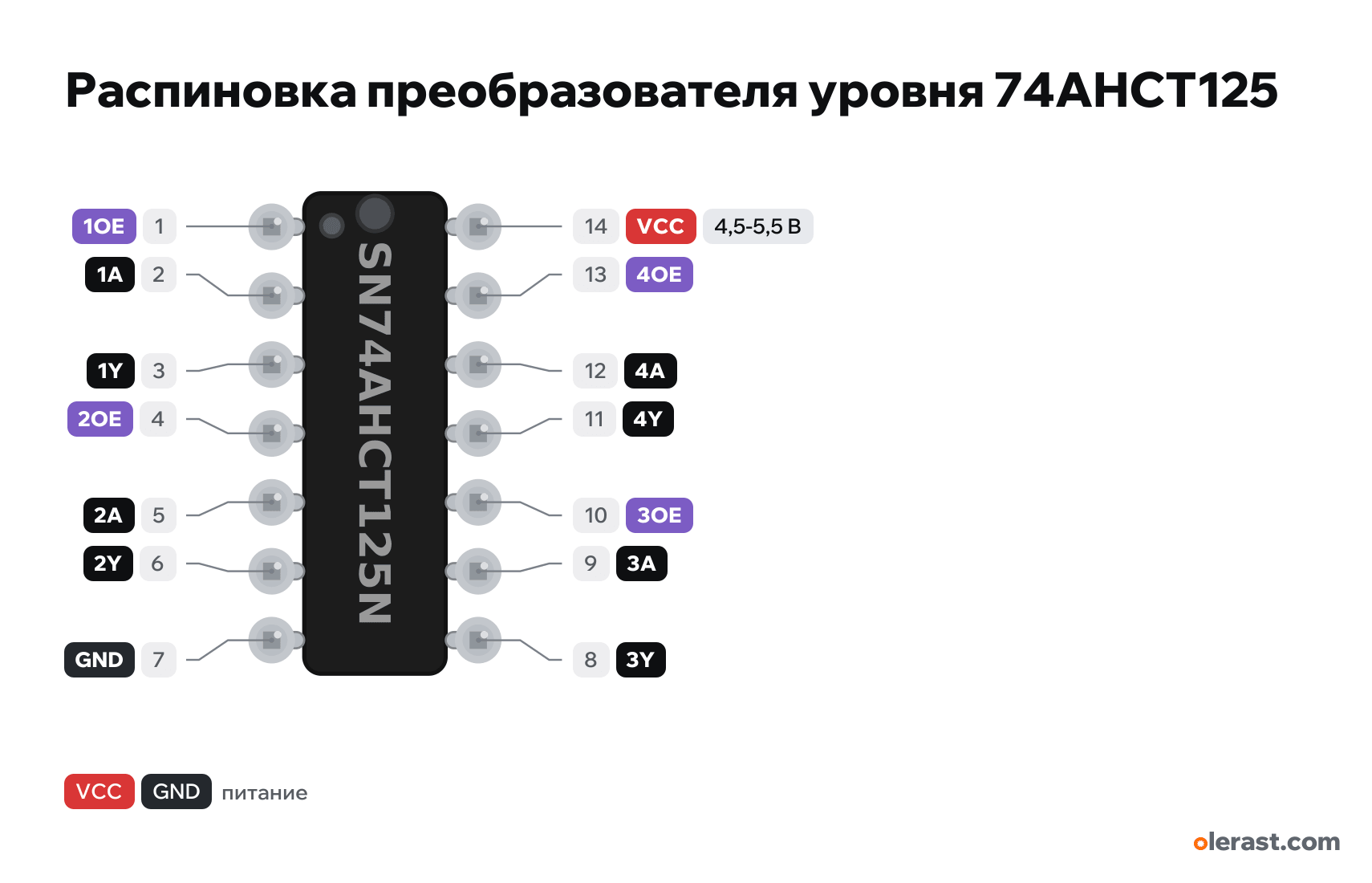
74AHCT125 buffer pinout
74AHCT125 buffer (DIP-14), 3.3 to 5 V level shifter, SN74AHCT125, 5 V logic, 18.32×9.7 mm, 14 pins
verified20.10.2026
Top view, notch on the left: pins 1-7 bottom left to right, 8-14 top right to left (14 above 1), rotated 90° on the diagram.
Download PNG- Chip
- SN74AHCT125
- Logic
- 5 V
- Power
- VCC (pin 14) 4.5-5.5 V
Important
- Why: the ESP32 and Pico output 3.3 V, while a WS2812B powered from 5 V reads a high from 3.5 V. A 5 V 74AHCT125 accepts 3.3 V as high (threshold 2 V) and outputs 5 V.
- Strip wiring: VCC (14) to 5 V, GND (7) to ground, 1OE (1) to GND, 1A (2) to the GPIO, 1Y (3) via 330 Ω to the strip DIN.
- Tie the unused inputs 2A, 3A, 4A and pins 2OE, 3OE, 4OE to GND: TI requires this, floating CMOS inputs draw extra current.
- One direction only (3.3 to 5 V). For I2C and other bidirectional lines you need a MOSFET level shifter (BSS138).
- Replacements: 74HCT125 and 74HCT245 (also TTL inputs). The 74HC125 without the T does not work: at a 5 V supply it needs a high from 3.5 V.
- Quiescent current 20 µA. Each input at 3.3 V adds up to 1.5 mA (TTL inputs).
Revisions and clones
- SOIC-14 (SN74AHCT125D), TSSOP-14: the same 1-14 order.
- 74AHCT1G125 (SOT-23-5): a single buffer, different pin order.
All pins
| Label | Number | Functions | Limits | Check |
|---|---|---|---|---|
| 1OE | pin 1 | 1OE: LOW enables output 1Y, HIGH disables it (third state) | verifiedLabelled on other revisions as: 1OE#, 1 | |
| 1A | pin 2 | 1A: input of buffer 1, threshold 2 V (accepts 3.3 V) | 5 V tolerant | verifiedLabelled on other revisions as: 2 |
| 1Y | pin 3 | 1Y: output of buffer 1, VCC level (5 V), up to 8 mA | verifiedLabelled on other revisions as: 3 | |
| 2OE | pin 4 | 2OE: LOW enables output 2Y, HIGH disables it (third state) | verifiedLabelled on other revisions as: 2OE#, 4 | |
| 2A | pin 5 | 2A: input of buffer 2, threshold 2 V (accepts 3.3 V) | 5 V tolerant | verifiedLabelled on other revisions as: 5 |
| 2Y | pin 6 | 2Y: output of buffer 2, VCC level (5 V), up to 8 mA | verifiedLabelled on other revisions as: 6 | |
| GND | pin 7 | Ground | verifiedLabelled on other revisions as: 7 | |
| 3Y | pin 8 | 3Y: output of buffer 3, VCC level (5 V), up to 8 mA | verifiedLabelled on other revisions as: 8 | |
| 3A | pin 9 | 3A: input of buffer 3, threshold 2 V (accepts 3.3 V) | 5 V tolerant | verifiedLabelled on other revisions as: 9 |
| 3OE | pin 10 | 3OE: LOW enables output 3Y, HIGH disables it (third state) | verifiedLabelled on other revisions as: 3OE#, 10 | |
| 4Y | pin 11 | 4Y: output of buffer 4, VCC level (5 V), up to 8 mA | verifiedLabelled on other revisions as: 11 | |
| 4A | pin 12 | 4A: input of buffer 4, threshold 2 V (accepts 3.3 V) | 5 V tolerant | verifiedLabelled on other revisions as: 12 |
| 4OE | pin 13 | 4OE: LOW enables output 4Y, HIGH disables it (third state) | verifiedLabelled on other revisions as: 4OE#, 13 | |
| VCC | pin 14 | 5 V | power input | verifiedLabelled on other revisions as: 14 |
Sources
Every pin is verified against the manufacturer's documents.
- TI SN54AHCT125, SN74AHCT125 Quadruple Bus Buffer Gates With 3-State Outputs (SCLS264R, February 2024)datasheet, checked 20.10.2026N (PDIP-14), top view: 1 1OE, 2 1A, 3 1Y, 4 2OE, 5 2A, 6 2Y, 7 GND, 8 3Y, 9 3A, 10 3OE, 11 4Y, 12 4A, 13 4OE, 14 VCC; VCC 4.5-5.5 V; VIH 2 V, VIL 0.8 V (TTL inputs); input up to 7 V; output ±8 mA; ICC 20 µA, plus up to 1.5 mA per input at 3.4 V; tie unused inputs to VCC or GND; OE low = output enabled
- Adafruit 1787: 74AHCT125 Quad Level-Shifter (3V to 5V)third-party source, checked 20.10.202674AHCT125 for shifting 3.3 V logic to 5 V for NeoPixel (WS2812); 5 V supply, treats 3.3 V as high on the inputs
Size: PDIP-14 package 19.3×6.35 mm, 2.54 pitch, rows 7.62 apart; the package is drawn narrower so the pins are visible (approximate).