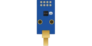
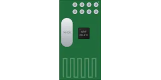
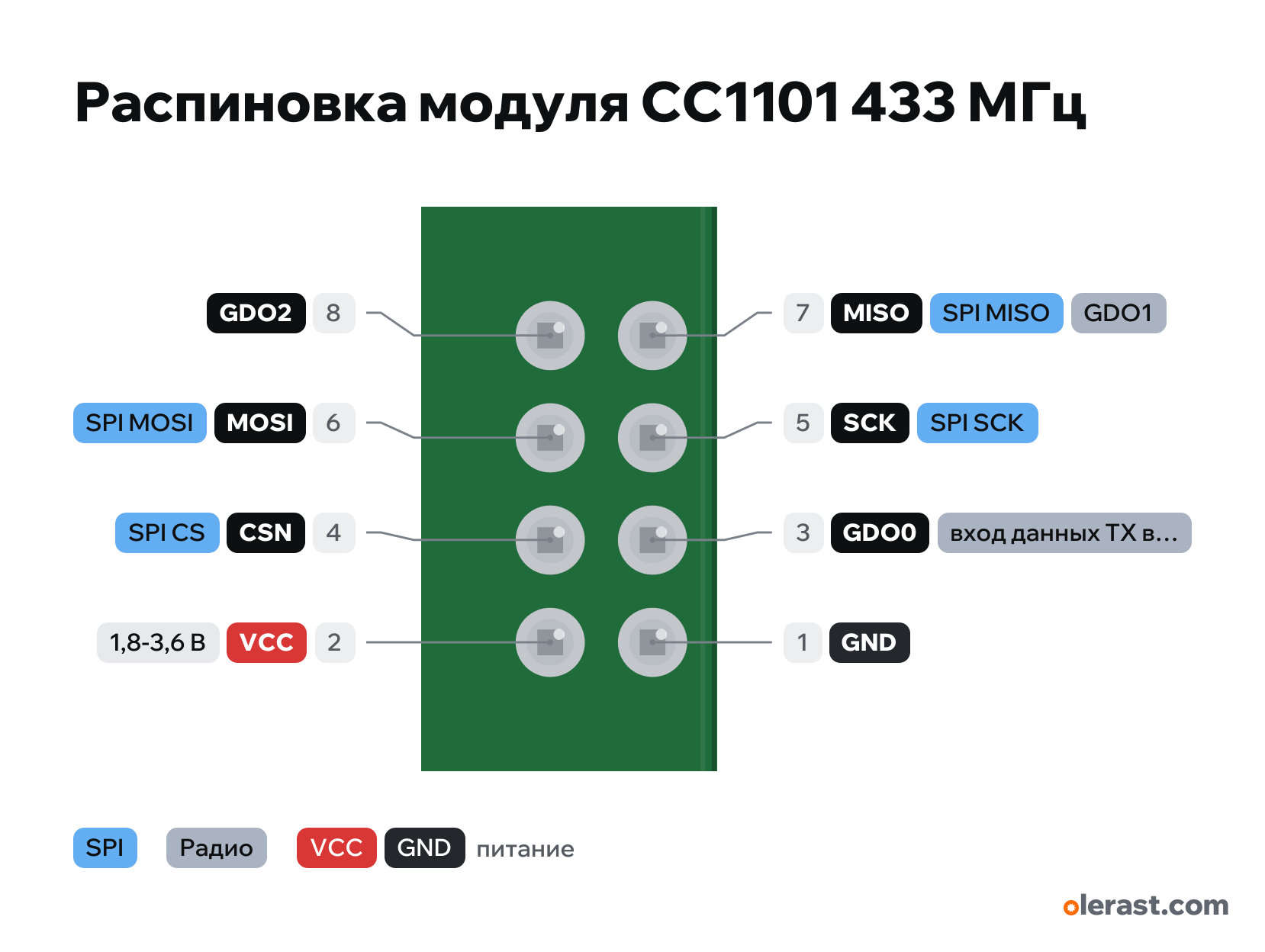
CC1101 green module 2×4 pinout
CC1101 green module 2×4 (433 MHz), CC1101 (TI), 3.3 V logic, 15×28 mm, 8 pins
partly verified15.10.2026
Top view (chip side), connector at the top, antenna at the bottom, rotated 90° on the diagram.
CompareDownload PNG- Chip
- CC1101 (TI)
- Logic
- 3.3 V
- Power
- VCC 1.8-3.6 V
Important
- Power and signals are 3.3 V only (TI: pins no higher than VDD+0.3 V). With an Arduino Uno, use a level shifter, otherwise the chip burns out.
- GDO0 and GDO2 are configurable outputs: packet-received interrupt, data in asynchronous mode. Usually GDO0 goes to the MCU interrupt pin, GDO2 can be left unconnected.
- The module is built for a single frequency (antenna matching network): 315, 433 or 868/915 MHz. Buy the one for your frequency.
- Check the labels on the board before connecting: incompatible 2×4 modules exist (for example 1 VCC, 2 GND, 3 MOSI…).
- ELECHOUSE says their module tolerates 5 V on the signals, but this contradicts the TI datasheet: assume it is not 5 V tolerant.
Revisions and clones
- ELECHOUSE CC1101 is another module with a 2×5 connector: 1, 2 VDD; 3 SI; 4 SCLK; 5 SO; 6 GDO2; 7 CSn; 8 GDO0; 9, 10 GND.
- Versions with SMA instead of the spring have the same pinout (if it is an E07 clone).
All pins
| Label | Number | Functions | Limits | Check |
|---|---|---|---|---|
| GND | pin 1 | Ground | not from manufacturerThere is no official manufacturer. The order 1 GND, 2 VCC, 3 GDO0, 4 CSN, 5 SCK, 6 MOSI, 7 MISO/GDO1, 8 GDO2 matches in five independent sources and on the Ebyte E07; the 2×4 layout is taken as on the E07. Some modules have a different order: check the labels on the board. | |
| VCC | pin 2 | 3.3 V | power input | not from manufacturerThere is no official manufacturer. The order 1 GND, 2 VCC, 3 GDO0, 4 CSN, 5 SCK, 6 MOSI, 7 MISO/GDO1, 8 GDO2 matches in five independent sources and on the Ebyte E07; the 2×4 layout is taken as on the E07. Some modules have a different order: check the labels on the board.1.8–3.6 V. 5 V will burn out the chip. |
| GDO0 | pin 3 | GDO0: configurable output (IOCFG0)usually to the MCU interrupt pinTX data input in asynchronous mode | not 5 V tolerant | not from manufacturerThere is no official manufacturer. The order 1 GND, 2 VCC, 3 GDO0, 4 CSN, 5 SCK, 6 MOSI, 7 MISO/GDO1, 8 GDO2 matches in five independent sources and on the Ebyte E07; the 2×4 layout is taken as on the E07. Some modules have a different order: check the labels on the board.After reset it outputs a CLK_XOSC/192 clock (~135 kHz); TI advises reconfiguring it at initialization. Libraries (SmartRC, ELECHOUSE) expect it on the interrupt pin, for example D2 on the Uno. |
| CSN | pin 4 | SPI CS (CSn, active low) | not 5 V tolerant | not from manufacturerThere is no official manufacturer. The order 1 GND, 2 VCC, 3 GDO0, 4 CSN, 5 SCK, 6 MOSI, 7 MISO/GDO1, 8 GDO2 matches in five independent sources and on the Ebyte E07; the 2×4 layout is taken as on the E07. Some modules have a different order: check the labels on the board. |
| SCK | pin 5 | SPI SCK (SCLK) | not 5 V tolerant | not from manufacturerThere is no official manufacturer. The order 1 GND, 2 VCC, 3 GDO0, 4 CSN, 5 SCK, 6 MOSI, 7 MISO/GDO1, 8 GDO2 matches in five independent sources and on the Ebyte E07; the 2×4 layout is taken as on the E07. Some modules have a different order: check the labels on the board. |
| MOSI | pin 6 | SPI MOSI (SI) | not 5 V tolerant | not from manufacturerThere is no official manufacturer. The order 1 GND, 2 VCC, 3 GDO0, 4 CSN, 5 SCK, 6 MOSI, 7 MISO/GDO1, 8 GDO2 matches in five independent sources and on the Ebyte E07; the 2×4 layout is taken as on the E07. Some modules have a different order: check the labels on the board. |
| MISO | pin 7 | SPI MISO (SO)GDO1 (when CSn is high) | not 5 V tolerant | not from manufacturerThere is no official manufacturer. The order 1 GND, 2 VCC, 3 GDO0, 4 CSN, 5 SCK, 6 MOSI, 7 MISO/GDO1, 8 GDO2 matches in five independent sources and on the Ebyte E07; the 2×4 layout is taken as on the E07. Some modules have a different order: check the labels on the board.Labelled on other revisions as: MISO/GDO1, SO |
| GDO2 | pin 8 | GDO2: configurable output (IOCFG2), CHP_RDYn after reset | not 5 V tolerant | not from manufacturerThere is no official manufacturer. The order 1 GND, 2 VCC, 3 GDO0, 4 CSN, 5 SCK, 6 MOSI, 7 MISO/GDO1, 8 GDO2 matches in five independent sources and on the Ebyte E07; the 2×4 layout is taken as on the E07. Some modules have a different order: check the labels on the board. |
Sources
Not verified against the manufacturer: 8 of 8 pins. The pin card says what confirms each one and where sources disagree.
- TI CC1101 Datasheet (SWRS061I)datasheet, checked 15.10.2026supply 1.8–3.6 V; digital pins no higher than VDD+0.3 V (3.9 V max), so not 5 V tolerant; SCLK, SI, SO/GDO1, CSn, GDO0, GDO2; GDO state after reset; bands 300–348, 387–464, 779–928 MHz
- Bastelgarage: CC1101 433MHz radio modulethird-party source, checked 15.10.2026pin order 1–8, supply 1.8–3.6 V
- Zaitronics: CC1101 guide / instruction manualthird-party source, checked 15.10.2026same order; 5 V on any pin kills the chip
- ESPHome: CC1101 componentthird-party source, checked 15.10.2026GDO0 is module pin 3, GDO2 is pin 8
- done.land: E07-M1101D / CC1101 transceiverthird-party source, checked 15.10.2026same order, size 15×28/38 mm
- IthoEcoFanRFT: another 2×4 CC1101 module (868 MHz)third-party source, checked 15.10.2026an incompatible 2×4 module exists: 1 VCC, 2 GND, 3 MOSI, 4 SCK, 5 MISO, 6 GDO2, 7 GDO0, 8 CSN
- Ebyte E07-M1101D-SMA User Manual v1.4datasheet, checked 15.10.2026same pin order and 2×4 grid on the branded module
Size: same as Ebyte E07 (sellers list 15×28–38 mm) (approximate).
FAQ
- What supply voltage does the CC1101 green module 2×4 need?
- VCC: 1.8-3.6 V. 3.3 V logic.