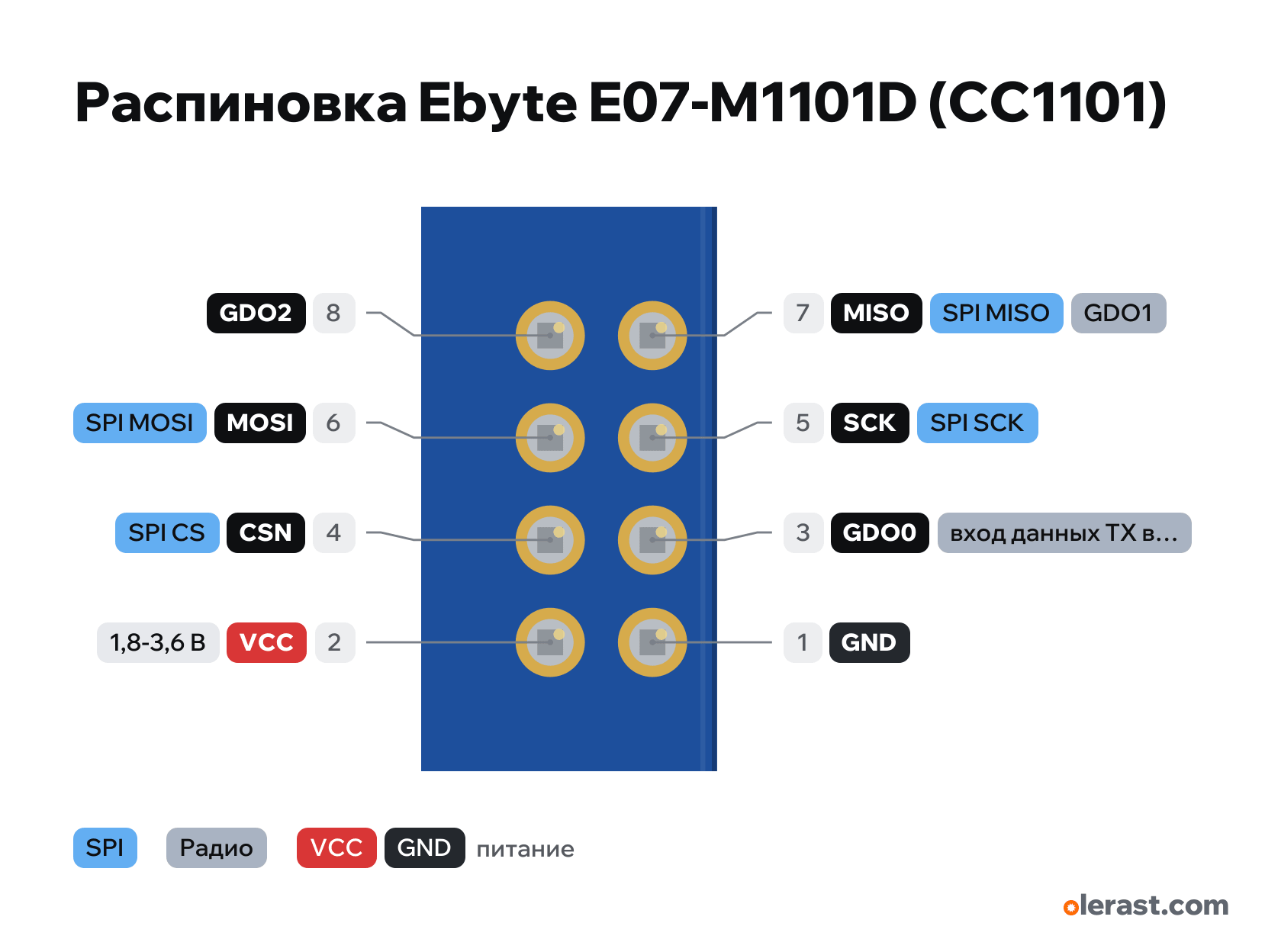
Ebyte E07-M1101D (CC1101) pinout
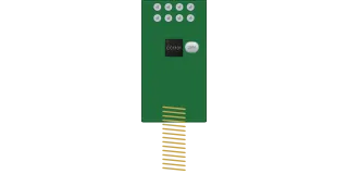
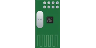
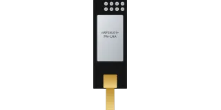
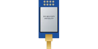
Ebyte E07-M1101D-SMA (CC1101, 433 MHz), CC1101 (TI), 3.3 V logic, 15×28 mm, 8 pins
verified15.10.2026
Top view (chip side), header at the top, SMA at the bottom, rotated 90° on the diagram.
CompareDownload PNG- Chip
- CC1101 (TI)
- Logic
- 3.3 V
- Power
- VCC 1.8-3.6 V
Important
- Power and signals are 3.3 V only (TI: pins no higher than VDD+0.3 V). With an Arduino Uno, use a level shifter, otherwise the chip burns out.
- GDO0 and GDO2 are configurable outputs: packet-received interrupt, data in asynchronous mode. Usually GDO0 goes to the MCU interrupt pin, GDO2 can be left unconnected.
- The module is built for a single frequency (antenna matching network): 315, 433 or 868/915 MHz. Buy the one for your frequency.
- Pins 9 and 10 are large mounting holes (GND); their vertical position is inconsistent in the manual and approximate in the drawing.
- Receive current 20 mA. Transmit current is 100 mA in the SMA version's manual and 29 mA in the TH version's at the same power (probably an error in the manual).
Revisions and clones
- E07-M1101D-TH: the same board with a spring antenna instead of SMA (30 mm long per the drawing, 28 in the table).
- For 868/915 MHz Ebyte has other models (E07-900M10S, SMD).
All pins
| Label | Number | Functions | Limits | Check |
|---|---|---|---|---|
| GND | pin 1 | Ground | verified | |
| VCC | pin 2 | 3.3 V | power input | verified1.8–3.6 V. 5 V will burn out the chip. |
| GDO0 | pin 3 | GDO0: configurable output (IOCFG0)usually to the MCU interrupt pinTX data input in asynchronous mode | not 5 V tolerant | verifiedAfter reset it outputs a CLK_XOSC/192 clock (~135 kHz); TI advises reconfiguring it at initialization. Libraries (SmartRC, ELECHOUSE) expect it on the interrupt pin, for example D2 on the Uno. |
| CSN | pin 4 | SPI CS (CSn, active low) | not 5 V tolerant | verified |
| SCK | pin 5 | SPI SCK (SCLK) | not 5 V tolerant | verified |
| MOSI | pin 6 | SPI MOSI (SI) | not 5 V tolerant | verified |
| MISO | pin 7 | SPI MISO (SO)GDO1 (when CSn is high) | not 5 V tolerant | verifiedLabelled on other revisions as: MISO/GDO1, SO |
| GDO2 | pin 8 | GDO2: configurable output (IOCFG2), CHP_RDYn after reset | not 5 V tolerant | verified |
Sources
Every pin is verified against the manufacturer's documents.
- TI CC1101 Datasheet (SWRS061I)datasheet, checked 15.10.2026supply 1.8–3.6 V; digital pins no higher than VDD+0.3 V (3.9 V max), so not 5 V tolerant; SCLK, SI, SO/GDO1, CSn, GDO0, GDO2; GDO state after reset; bands 300–348, 387–464, 779–928 MHz
- Ebyte E07-M1101D-SMA User Manual v1.4 (2023-10-24)datasheet, checked 15.10.2026size 15.0×28.0 mm, 2×4 header (pin 1 is 3.70 and 1.60 mm from the edges in the bottom view), pins 1–10 functions, supply 1.8–3.6 V, 3.3 V level
- Ebyte E07-M1101D-TH User Manual v1.30 (2021-03-11)datasheet, checked 15.10.2026same pinout and header grid, 25 mm spring antenna, TX 29 mA
Size: from the Ebyte drawing (37.6 mm with SMA).
FAQ
- What supply voltage does the Ebyte E07-M1101D (CC1101) need?
- VCC: 1.8-3.6 V. 3.3 V logic.