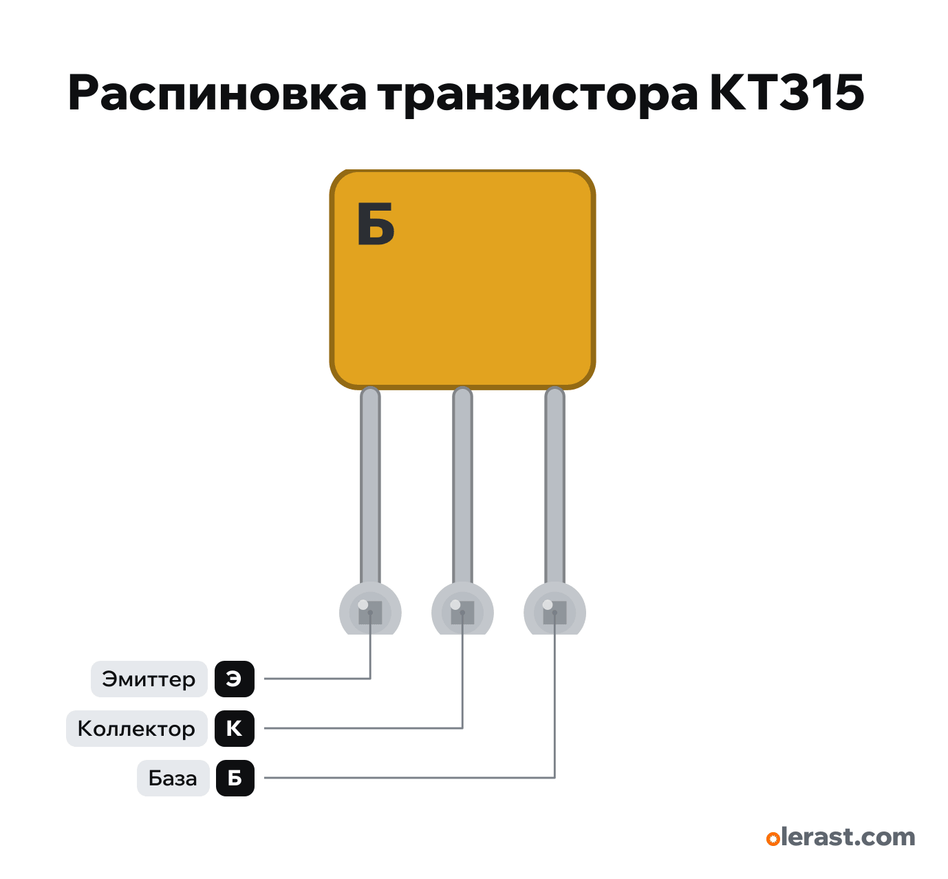
KT315 transistor pinout
KT315 transistor (NPN, KT-13 package), KT315, 5 V logic, 7.6×12.8 mm, 3 pins
partly verified20.10.2026
View of the flat side with the letter, pins down: E, C, B from left to right.
Download PNG- Chip
- KT315
- Logic
- 5 V
Important
- Low-side switch (NPN): E to GND, load between the positive rail and C, B through 1-4.7 kΩ to a GPIO. From the 3.3 V of an ESP32 through 1 kΩ the base current is about 2.6 mA: with the worst-case h21e of 20 that is 50 mA of load.
- Collector current up to 100 mA (KT315Zh and KT315I up to 50 mA): LEDs, small relays, buzzers. Motors and high-current relays go through a MOSFET.
- Collector-emitter voltage by letter suffix: B and Zh 20 V, A 25 V, G, E and R 35 V, V and D 40 V, I 60 V. Power up to 150 mW: no heatsink.
- PNP complement: KT361 in the same package.
- Multimeter diode-mode test: positive probe on B, negative probe on E and C in turn, both junctions conduct; between E and C there is no reading in either direction. Tell the emitter from the collector by the drawing.
Revisions and clones
- KT315 in the KT-26 package (TO-92, "Integral"): 1 base, 2 collector, 3 emitter, B-C-E when viewed from the flat side, the reverse of KT-13. A letter with a digit in the marking (KT315G1, etc.) means a different package: check the datasheet.
- KT361 (PNP): the group letter is in the middle of the upper part of the flat side.
All pins
| Label | Number | Functions | Limits | Check |
|---|---|---|---|---|
| E | Emitter: to GND | not from manufacturerThe E-C-B order comes from the KT-13 drawing in the reference book; I found no manufacturer document with the KT-13 pinout online. The view side is inferred from the drawing (left view to the right of the main one, bevel on the back side) and from the letter being on the flat side. Test with a meter before soldering: the base conducts in one direction to both other pins.Labelled on other revisions as: E, emitter | ||
| C | Collector: load negative | not from manufacturerThe E-C-B order comes from the KT-13 drawing in the reference book; I found no manufacturer document with the KT-13 pinout online. The view side is inferred from the drawing (left view to the right of the main one, bevel on the back side) and from the letter being on the flat side. Test with a meter before soldering: the base conducts in one direction to both other pins.Labelled on other revisions as: C, collector | ||
| B | Base: through a 1-4.7 kΩ resistor to a GPIO | not from manufacturerThe E-C-B order comes from the KT-13 drawing in the reference book; I found no manufacturer document with the KT-13 pinout online. The view side is inferred from the drawing (left view to the right of the main one, bevel on the back side) and from the letter being on the flat side. Test with a meter before soldering: the base conducts in one direction to both other pins.Labelled on other revisions as: B, base |
Sources
Not verified against the manufacturer: 3 of 3 pins. The pin card says what confirms each one and where sources disagree.
- KT315A-KT315R, reference data with the package drawing (copy from "Elektronika i Svyaz")third-party source, checked 20.10.2026KT-13 drawing: on the main view emitter on the left, collector in the middle, base on the right, 2.5 mm pitch, 7.2×3 mm body; manufacturers "Kremniy", Nalchik, Tomsk; h21e 20-350 by letter suffix, fT from 250 MHz
- KT315A-KT315R: specifications, KT-13 package, TU ZhK3.365.200 (ChipDip)third-party source, checked 20.10.2026Ic max 100 mA (Zh, I 50 mA); UceR max: A 25, B 20, V 40, G 35, D 40, E 35, Zh 20, I 60, R 35 V; Pc 150 mW (Zh, I 100 mW); KT-13 package
- "Integral" KT315, silicon NPN transistor (rev. 1.1, May 2012)datasheet, checked 20.10.2026KT-26 package (TO-92): pin 1 base, 2 collector, 3 emitter; prototype 2SC544-2SC546; TU ZhK3.365.200 TU/02
- Wikipedia: KT315third-party source, checked 20.10.2026KT-13 package, group letter in the top left corner of the flat side; the KT361 PNP complement comes in the same package; later versions in KT-26
Size: KT-13 package 7.2×3 mm, pin pitch 2.5 mm (drawn at 2.54) (approximate).