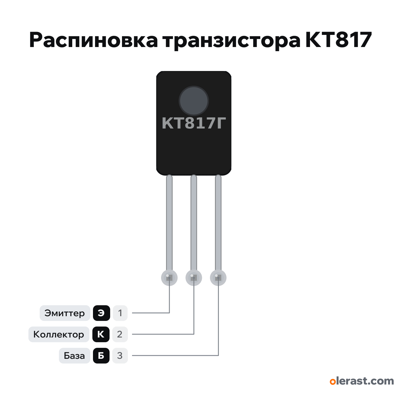
KT817 transistor pinout
KT817 transistor (n-p-n, 3 A, KT-27 package), KT817, 5 V logic, 7.8×23 mm, 3 pins
partly verified20.10.2026
View of the marked side, hole at the top, leads down: 1 E, 2 C, 3 B from left to right.
Download PNG- Chip
- KT817
- Logic
- 5 V
Important
- Low-side switch: E to GND, load between plus and C, B through a resistor to a GPIO. The base current must be large: at h21e from 25 a 1 A load needs 40 mA of base current, while a GPIO gives 20 mA. For currents above 0.3-0.5 A from a GPIO use a Darlington transistor (KT829, TIP120) or a logic-level MOSFET (IRLZ44N).
- Base resistor from 3.3 V: (3.3 − 0.7) / 0.015 ≈ 170 Ω for a base current of 15 mA, which is enough for about a 375 mA load at h21e 25.
- Without a heatsink up to 1 W: at saturation of 0.5-1 V this is about 1-2 A. The metal side of the package is connected to the collector, use an insulating pad for the heatsink.
- Voltage by letter: A 25-40 V, B 45 V, V 60 V, G 80-90 V (sources disagree, use the lower value).
- p-n-p counterpart: KT816 in the same package. Foreign equivalents: BD139 (same E-C-B order), TIP31 (different package and order).
Revisions and clones
- Some manufacturers make the KT817 in KT-28 (TO-220): check the pin order against the document.
- KT815 (1.5 A) and KT819 (10 A): similar n-p-n transistors, each with its own package and pin order.
All pins
| Label | Number | Functions | Limits | Check |
|---|---|---|---|---|
| E | pin 1 | Emitter: to GND | not from manufacturerI did not find a manufacturer document online: the order 1 E, 2 C, 3 B is from a reference book drawing. Sources give the KT817A voltage as 25 or 40 V and KT817G as 80 or 90 V: the lower value is used in the data. Check with a multimeter before soldering.Labelled on other revisions as: E, emitter, 1 | |
| C | pin 2 | Collector: load minus (and the metal side) | not from manufacturerI did not find a manufacturer document online: the order 1 E, 2 C, 3 B is from a reference book drawing. Sources give the KT817A voltage as 25 or 40 V and KT817G as 80 or 90 V: the lower value is used in the data. Check with a multimeter before soldering.Labelled on other revisions as: C, collector, 2 | |
| B | pin 3 | Base: through a resistor to a GPIO | not from manufacturerI did not find a manufacturer document online: the order 1 E, 2 C, 3 B is from a reference book drawing. Sources give the KT817A voltage as 25 or 40 V and KT817G as 80 or 90 V: the lower value is used in the data. Check with a multimeter before soldering.Labelled on other revisions as: B, base, 3 |
Sources
Not verified against the manufacturer: 3 of 3 pins. The pin card says what confirms each one and where sources disagree.
- RadioLibrary: KT817A, KT817B, KT817V, KT817G transistors (package drawing and pin assignment)third-party source, checked 20.10.2026drawing: package 7.8×10.8×2.8 mm, leads 16 mm, 1 E, 2 C, 3 B; n-p-n; Ic 3 A (6 A pulse); Pc 1 W without a heatsink, 25 W with a heatsink; h21e 25-275; fT from 3 MHz; Uce: A 40, B 45, V 60, G 90 V (pulse)
Size: KT-27 package 7.8×10.8×2.8 mm, leads 16 mm shortened, 2.3 mm pitch (drawn at 2.54) (approximate).