S8550 transistor pinout
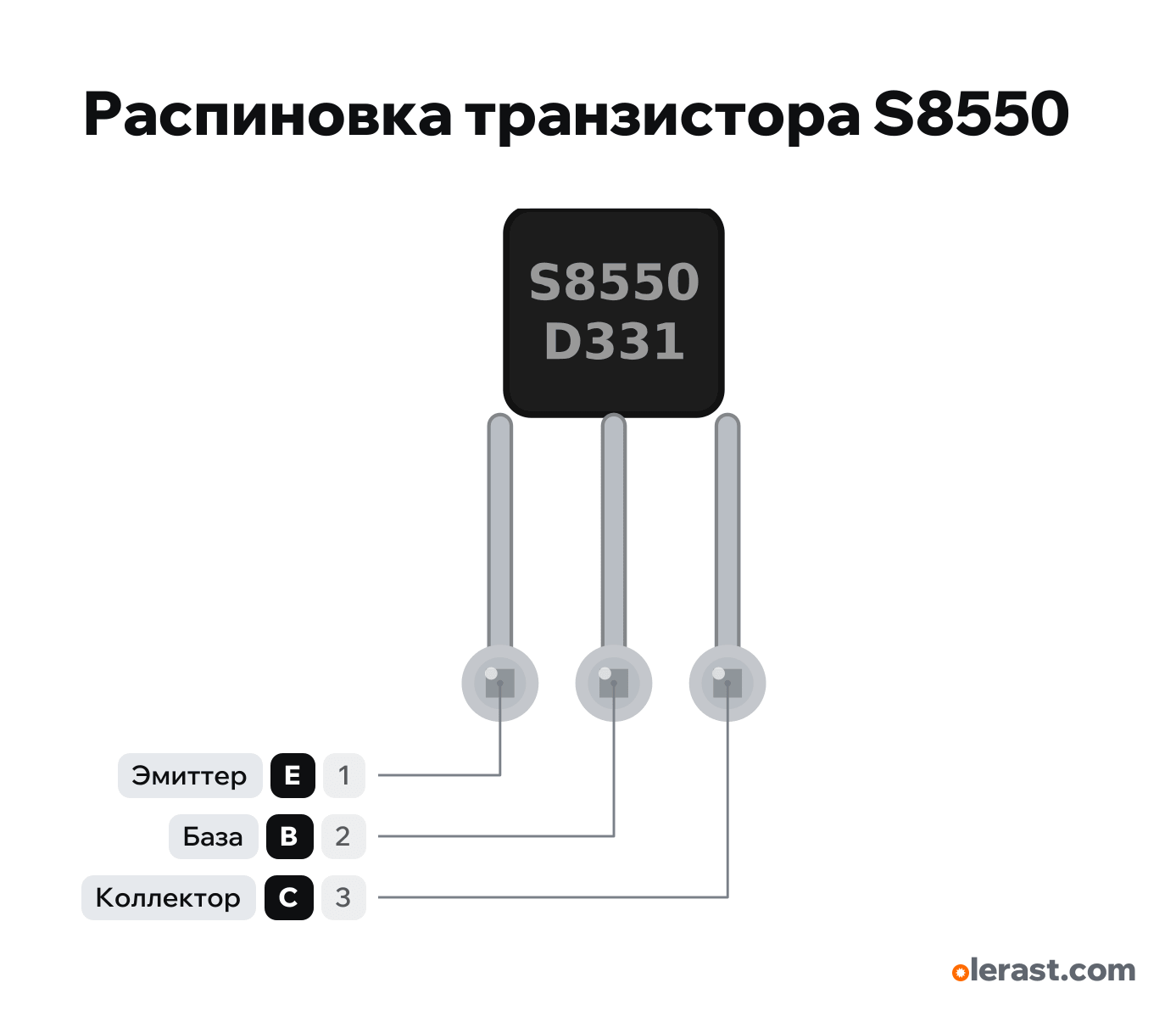
S8550 transistor (PNP, TO-92, E-B-C), S8550 D331, 5 V logic, 7.2×11.5 mm, 3 pins
partly verified17.10.2026
View of the flat marked side, pins down: E-B-C left to right.
Download PNG- Chip
- S8550 D331
- Logic
- 5 V
Important
- High-side switch (PNP): emitter to the positive supply, load between the collector and GND, base through a resistor to a GPIO, turns on with LOW. If the supply is higher than the pin's logic level (5 V with a 3.3 V ESP32), the PNP won't turn off: add an extra NPN.
- Used on buzzer modules with an active low level (I/O = LOW sounds).
Revisions and clones
- 8550S (JCET): E-C-B.
All pins
| Label | Number | Functions | Limits | Check |
|---|---|---|---|---|
| E | pin 1 | Emitter: to the positive supply | not from manufacturerThe E-B-C order is taken from the onsemi SS8550 and the JCET S8050 pair; the JCET S8550 datasheet itself could not be downloaded. The 8550S (JCET) is E-C-B.Labelled on other revisions as: emitter, 1 | |
| B | pin 2 | Base: through a 1–10 kΩ resistor to a GPIO (a PNP turns on with a low level) | not from manufacturerThe E-B-C order is taken from the onsemi SS8550 and the JCET S8050 pair; the JCET S8550 datasheet itself could not be downloaded. The 8550S (JCET) is E-C-B.Labelled on other revisions as: base, 2 | |
| C | pin 3 | Collector | not from manufacturerThe E-B-C order is taken from the onsemi SS8550 and the JCET S8050 pair; the JCET S8550 datasheet itself could not be downloaded. The 8550S (JCET) is E-C-B.Labelled on other revisions as: collector, 3 |
Sources
Not verified against the manufacturer: 3 of 3 pins. The pin card says what confirms each one and where sources disagree.
- onsemi SS8550 PNP Epitaxial Silicon Transistor (Rev. 3, August 2021)datasheet, checked 17.10.2026TO-92: 1 Emitter, 2 Base, 3 Collector; −25 V, −1.5 A
Size: TO-92 package 4.8×4.6 mm, leads spread to 2.54 mm pitch (the package pitch is 1.27 mm) (approximate).