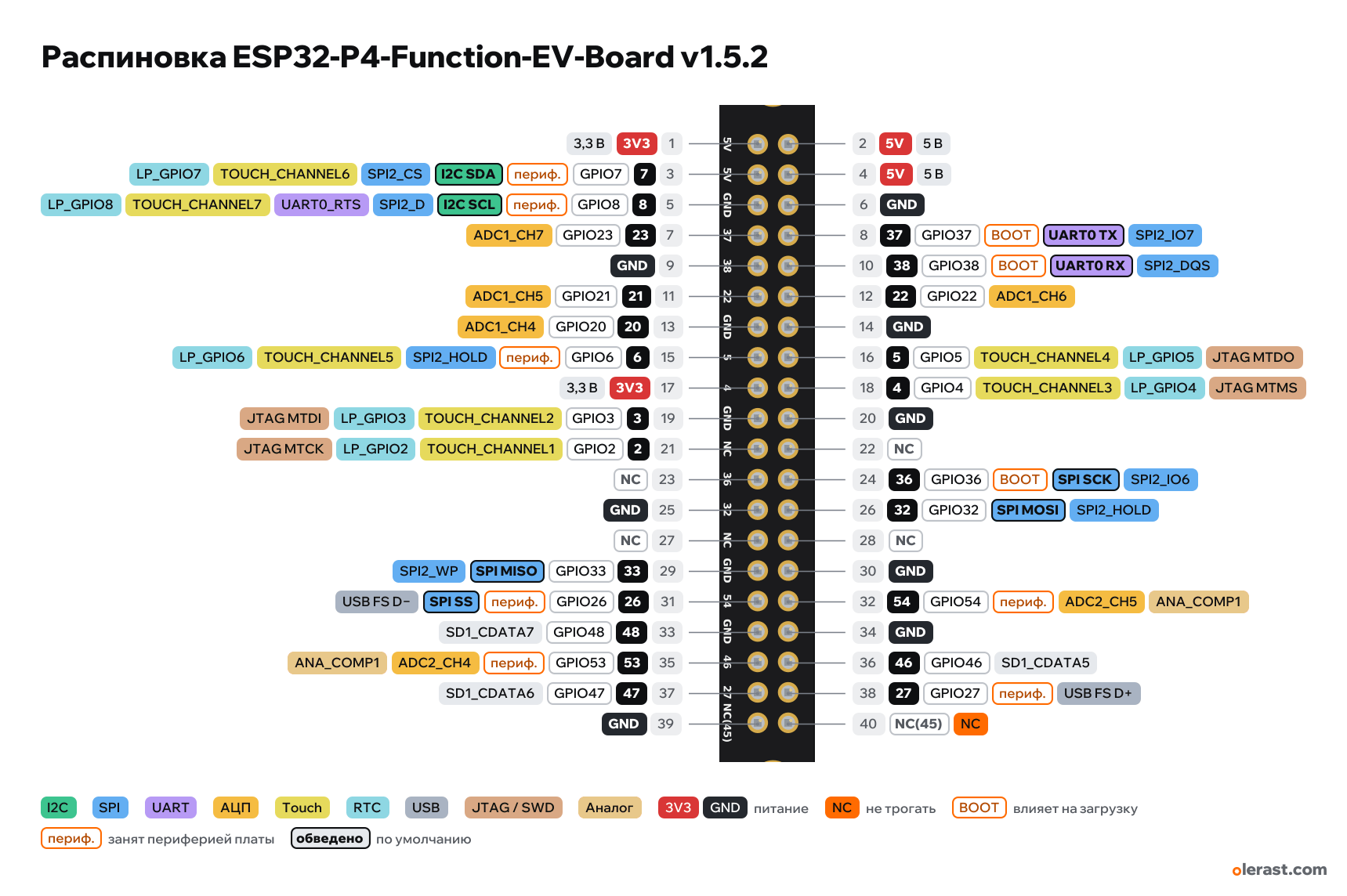
ESP32-P4-Function-EV-Board v1.5.2 pinout
ESP32-P4-Function-EV-Board v1.5.2, ESP32-P4, 3.3 V logic, 88×74 mm, 40 pins
verified20.10.2026
- 13V33.3 V
- 37GPIO7periph.I2C SDASPI2_CSTOUCH_CHANNEL6LP_GPIO7
- 58GPIO8periph.I2C SCLSPI2_DUART0_RTSTOUCH_CHANNEL7LP_GPIO8
- 723GPIO23ADC1_CH7
- 9GND
- 1121GPIO21ADC1_CH5
- 1320GPIO20ADC1_CH4
- 156GPIO6periph.SPI2_HOLDTOUCH_CHANNEL5LP_GPIO6
- 173V33.3 V
- 193GPIO3TOUCH_CHANNEL2LP_GPIO3JTAG MTDI
- 212GPIO2TOUCH_CHANNEL1LP_GPIO2JTAG MTCK
- 23NC
- 25GND
- 27NC
- 2933GPIO33SPI MISOSPI2_WP
- 3126GPIO26periph.SPI SSUSB FS D−
- 3348GPIO48SD1_CDATA7
- 3553GPIO53periph.ADC2_CH4ANA_COMP1
- 3747GPIO47SD1_CDATA6
- 39GND
- 25V5 V
- 45V5 V
- 6GND
- 837GPIO37BOOTUART0 TXSPI2_IO7
- 1038GPIO38BOOTUART0 RXSPI2_DQS
- 1222GPIO22ADC1_CH6
- 14GND
- 165GPIO5TOUCH_CHANNEL4LP_GPIO5JTAG MTDO
- 184GPIO4TOUCH_CHANNEL3LP_GPIO4JTAG MTMS
- 20GND
- 22NC
- 2436GPIO36BOOTSPI SCKSPI2_IO6
- 2632GPIO32SPI MOSISPI2_HOLD
- 28NC
- 30GND
- 3254GPIO54periph.ADC2_CH5ANA_COMP1
- 34GND
- 3646GPIO46SD1_CDATA5
- 3827GPIO27periph.USB FS D+
- 40NC(45)NC
Top view, header J1 at the top edge, USB-C and Ethernet at the bottom, rotated 90° on the diagram.
CompareDownload PNG- Chip
- ESP32-P4, ESP32-C6-MINI-1 (Wi-Fi 6 and Bluetooth LE for the P4 over SDIO)
- Logic
- 3.3 V
- Power
- USB-C (USB HS, USB Serial/JTAG or USB FS) 4.75-5.25 V5V 4.75-5.25 V
- Defaults in arduino-esp32 (variants/esp32p4)
- I2C: SDA 7, SCL 8SPI: MOSI 32, MISO 33, SCK 36, SS 26UART: TX 37, RX 38
Which ESP32-P4-Function-EV-Board v1.5.2 pins are safe to use
Free to use
GPIO2-5, GPIO20-23, GPIO32, GPIO33, GPIO46-48
Use with care
- GPIO6-8, GPIO26, GPIO27, GPIO53, GPIO54: onboard peripherals are wired to them.
- GPIO36-38: strapping: the level at power-up selects the boot mode.
Important
- 3.3 V logic, do not apply 5 V to GPIO. GPIO46-48 are powered by the internal LDO_VO4: 1.8 or 3.3 V depending on its setting.
- The ESP32-P4 has no Wi-Fi or Bluetooth: the radio on the board is the ESP32-C6-MINI-1 module, connected over SDIO.
- Used by board peripherals and brought out to J1: GPIO7/8 (I2C for codec, camera and display), GPIO6 and 54 (ESP32-C6 module), GPIO53 (amplifier), GPIO26/27 (USB FS port).
- Strapping pins on J1: GPIO36, 37, 38. GPIO35 (BOOT button) is not brought out to the header.
- NC(1), NC(0), NC(45): GPIO1, GPIO0 and GPIO45 are used by default (32 kHz crystal, memory card power) and are freed by moving resistors.
- Flashing goes through the USB Serial/JTAG port (J19). UART0 (GPIO37/38) is only on J1.
- J1 pitch 2.54, mounting holes 58×49 mm.
- Small components are drawn approximately; the header, holes and outline follow the dimension drawing.
- Switch SW3 (OFF/ON) sits between USB and the VCC_5V rail. 3.3 V comes from the TLV62569 DC-DC (2 A per the schematic).
Revisions and clones
- v1.4: J1 also had IO24 and IO25, debugging went through a USB-UART bridge on USB-C. In v1.5.2 it is replaced by the chip's own USB Serial/JTAG (GPIO24/25) and a new USB FS port (GPIO26/27).
All pins
| Label | Number | Functions | Limits | Check |
|---|---|---|---|---|
| 3V3 | pin 1 | 3.3 V | power output | verifiedTLV62569 DC-DC output (ESP_3V3 net). |
| 5V | pin 2 | 5 V | power inputpower output | verifiedVCC_5V net: 5 V from USB-C after switch SW3. |
| 7 | GPIO7, pin 3 | interruptPWM (LEDC)LP_GPIO7TOUCH_CHANNEL6SPI2_CSI2C SDA | not 5 V tolerantused by onboard peripherals (camera, card, display) | verifiedBoard I2C bus (ESP_I2C_SDA): ES8311 codec, camera and display connectors. |
| 5V | pin 4 | 5 V | power inputpower output | verifiedVCC_5V net. |
| 8 | GPIO8, pin 5 | interruptPWM (LEDC)LP_GPIO8TOUCH_CHANNEL7SPI2_DUART0_RTSI2C SCL | not 5 V tolerantused by onboard peripherals (camera, card, display) | verifiedBoard I2C bus (ESP_I2C_SCL): ES8311 codec, camera and display connectors. |
| GND | pin 6 | Ground | verified | |
| 23 | GPIO23, pin 7 | interruptPWM (LEDC)ADC1_CH7 | not 5 V tolerant | verified |
| 37 | GPIO37, pin 8 | interruptPWM (LEDC)UART0 TXSPI2_IO7 (IO MUX) | not 5 V tolerantaffects boot (strapping)outputs a signal at boot | verifiedStrapping pin: takes part in boot mode selection (GPIO35-38). On the board it is also tied to the GPIO37_BOOTMODE net.Labelled on other revisions as: U0TXD |
| GND | pin 9 | Ground | verified | |
| 38 | GPIO38, pin 10 | interruptPWM (LEDC)UART0 RXSPI2_DQS (IO MUX) | not 5 V tolerantaffects boot (strapping) | verifiedStrapping pin: takes part in boot mode selection (GPIO35-38). On the board it is also tied to the GPIO38_BOOTMODE net.Labelled on other revisions as: U0RXD |
| 21 | GPIO21, pin 11 | interruptPWM (LEDC)ADC1_CH5 | not 5 V tolerant | verified |
| 22 | GPIO22, pin 12 | interruptPWM (LEDC)ADC1_CH6 | not 5 V tolerant | verified |
| 20 | GPIO20, pin 13 | interruptPWM (LEDC)ADC1_CH4 | not 5 V tolerant | verified |
| GND | pin 14 | Ground | verified | |
| 6 | GPIO6, pin 15 | interruptPWM (LEDC)LP_GPIO6TOUCH_CHANNEL5SPI2_HOLD | not 5 V tolerantused by onboard peripherals (camera, card, display) | verifiedConnected to the ESP32-C6 module (C6_WAKEUP net). |
| 5 | GPIO5, pin 16 | interruptPWM (LEDC)LP_GPIO5JTAG MTDOTOUCH_CHANNEL4 | not 5 V tolerant | verifiedJTAG pins (IO MUX). You can leave them free for debugging: JTAG is available through the USB Serial/JTAG port. |
| 3V3 | pin 17 | 3.3 V | power output | verified |
| 4 | GPIO4, pin 18 | interruptPWM (LEDC)LP_GPIO4JTAG MTMSTOUCH_CHANNEL3 | not 5 V tolerant | verifiedJTAG pins (IO MUX). You can leave them free for debugging: JTAG is available through the USB Serial/JTAG port. |
| 3 | GPIO3, pin 19 | interruptPWM (LEDC)LP_GPIO3JTAG MTDITOUCH_CHANNEL2 | not 5 V tolerant | verifiedJTAG pins (IO MUX). You can leave them free for debugging: JTAG is available through the USB Serial/JTAG port. |
| GND | pin 20 | Ground | verified | |
| 2 | GPIO2, pin 21 | interruptPWM (LEDC)LP_GPIO2JTAG MTCKTOUCH_CHANNEL1 | not 5 V tolerant | verifiedJTAG pins (IO MUX). You can leave them free for debugging: JTAG is available through the USB Serial/JTAG port. |
| NC | pin 22 | not connected | verifiedGPIO1 is used by the 32 kHz crystal by default. It appears on J1 after moving R59 to R197.Labelled on other revisions as: NC(1) | |
| NC | pin 23 | not connected | verifiedGPIO0 is used by the 32 kHz crystal by default. It appears on J1 after moving R61 to R199.Labelled on other revisions as: NC(0) | |
| 36 | GPIO36, pin 24 | interruptPWM (LEDC)SPI2_IO6 (IO MUX)SPI SCK | not 5 V tolerantaffects boot (strapping) | verifiedStrapping pin: boot mode (together with GPIO35) and ROM log output. Weak internal pull-up; it must be high at reset to enter download mode. |
| GND | pin 25 | Ground | verified | |
| 32 | GPIO32, pin 26 | interruptPWM (LEDC)SPI2_HOLD (IO MUX)SPI MOSI | not 5 V tolerant | verified |
| NC | pin 27 | not connected | verified | |
| NC | pin 28 | not connected | verified | |
| 33 | GPIO33, pin 29 | interruptPWM (LEDC)SPI2_WP (IO MUX)SPI MISO | not 5 V tolerant | verified |
| GND | pin 30 | Ground | verified | |
| 26 | GPIO26, pin 31 | interruptPWM (LEDC)USB FS D− (USB1P1_N1)SPI SS | not 5 V tolerantused by onboard peripherals (camera, card, display) | verifiedAlso goes through 33 Ω to the USB FS port (J20, D−). The pin is taken while the port is in use. |
| 54 | GPIO54, pin 32 | interruptPWM (LEDC)ADC2_CH5ANA_COMP1 (comparator) | not 5 V tolerantused by onboard peripherals (camera, card, display) | verifiedConnected to the EN pin of the ESP32-C6 module (C6_EN net). |
| 48 | GPIO48, pin 33 | interruptPWM (LEDC)SD1_CDATA7 | not 5 V tolerant | verifiedThe GPIO39-48 group is powered by the internal LDO_VO4 (net 1V8/3V3 SDIO on the schematic): pin level is 1.8 or 3.3 V depending on the LDO setting. |
| GND | pin 34 | Ground | verified | |
| 53 | GPIO53, pin 35 | interruptPWM (LEDC)ADC2_CH4ANA_COMP1 (comparator) | not 5 V tolerantused by onboard peripherals (camera, card, display) | verifiedEnables the NS4150B amplifier (PA_CTRL net). |
| 46 | GPIO46, pin 36 | interruptPWM (LEDC)SD1_CDATA5 | not 5 V tolerant | verifiedThe GPIO39-48 group is powered by the internal LDO_VO4 (net 1V8/3V3 SDIO on the schematic): pin level is 1.8 or 3.3 V depending on the LDO setting. |
| 47 | GPIO47, pin 37 | interruptPWM (LEDC)SD1_CDATA6 | not 5 V tolerant | verifiedThe GPIO39-48 group is powered by the internal LDO_VO4 (net 1V8/3V3 SDIO on the schematic): pin level is 1.8 or 3.3 V depending on the LDO setting. |
| 27 | GPIO27, pin 38 | interruptPWM (LEDC)USB FS D+ (USB1P1_P1) | not 5 V tolerantused by onboard peripherals (camera, card, display) | verifiedAlso goes through 33 Ω to the USB FS port (J20, D+). The pin is taken while the port is in use. |
| GND | pin 39 | Ground | verified | |
| NC(45) | pin 40 | not connected | verifiedGPIO45 is used by the SD_PWRn net (memory card power) by default. It appears on J1 after moving R231 to R100. |
Sources
Every pin is verified against the manufacturer's documents.
- ESP32-P4-Function-EV-Board User Guide (Espressif), Header Block J1user guide, checked 20.10.2026function of the 40 J1 pins (v1.52), NC(0), NC(1), NC(45) and the R59/R197, R61/R199, R231/R100 resistor moves, power from three USB-C ports, differences from v1.4
- ESP32-P4-Function-EV-Board dimensions (PDF)board drawing, checked 20.10.202682.50 / 88.00 × 74.00 mm, protrusion 53.50; J1 rows 2.23 and 4.77 mm from the edge, first column 8.37 mm, pitch 2.54 (measured from the drawing); holes 3.5/61.5 × 3.5/52.5; J1 labels on the silkscreen
- ESP32-P4-Function-EV-Board schematic v1.52schematic, checked 20.10.2026J1: ESP_3V3, VCC_5V, CNN_GPIO; GPIO7/8 to ESP_I2C, GPIO6 to C6_WAKEUP, GPIO53 to PA_CTRL, GPIO54 to C6_EN, GPIO26/27 through 33 Ω to USB FS, GPIO45 to SD_PWRn, VDD_IO_5 from ESP_LDO_VO4 (1V8/3V3 SDIO), TLV62569, SW3
- ESP32-P4 Series Datasheet v0.7 (Espressif)datasheet, checked 20.10.2026IO MUX: JTAG on GPIO2-5, UART0 on GPIO37/38, SPI2 on GPIO6-8 and 32-38; analog: TOUCH_CHANNEL1-14 on GPIO2-15, ADC1_CH0-7 on GPIO16-23, ADC2_CH0-5 on GPIO49-54, USB FS on GPIO26/27; LP GPIO0-15; strapping GPIO34-38; VDD_IO_5 domain for GPIO39-48
- arduino-esp32: variants/esp32p4/pins_arduino.hArduino core, checked 20.10.2026defaults: TX 37, RX 38, SDA 7, SCL 8, SS 26, MOSI 32, MISO 33, SCK 36; GPIO39-48 from LDO VO4
Size: per the Espressif dimension drawing: 82.50 mm along the top edge, 88.00 along the bottom, 74.00 tall, lower protrusion 53.50.
FAQ
- Which ESP32-P4-Function-EV-Board v1.5.2 pins are I2C, SPI and UART?
- By default in arduino-esp32 (variants/esp32p4): I2C: SDA GPIO7, SCL GPIO8; SPI: MOSI GPIO32, MISO GPIO33, SCK GPIO36, SS GPIO26; UART: TX GPIO37, RX GPIO38.
- Are the ESP32-P4-Function-EV-Board v1.5.2 pins 5 V tolerant?
- No. The logic is 3.3 V and the pins are not 5 V tolerant: use a divider or a level shifter for 5 V signals.
You might also need
Schematic with this board
schematic builder with the board already placed
Flash this board
upload a sketch or .bin to this board from the browser
Power budget
will the regulator cope and how long the battery lasts
Calculators
LED resistor, voltage divider, battery runtime, 3D print cost, LED strip power supply and pF, nF, µF conversion
Similar boards
Next
- Emotion keychainmy ESP32-C5 project, prototype
- ESP32 music playermy ESP32 project, prototype
- DITHR//CAMmy ESP32 project, prototype
Need firmware or a device built on ESP32? I'll build it to order