ESP32-C5 DevKitC-1 pinout
ESP32-C5-DevKitC-1 v1.2, ESP32-C5, 3.3 V logic, 25.4×53.6 mm, 32 pins
verified15.10.2026
- 3V33.3 V
- RSTbuttonCHIP_PU
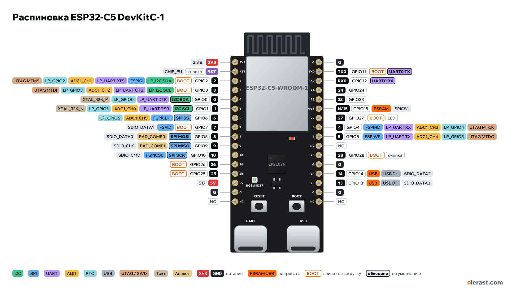
- 2GPIO2BOOTLP_I2C SDAFSPIQLP_UART RTSADC1_CH1LP_GPIO2JTAG MTMS
- 3GPIO3BOOTLP_I2C SCLLP_UART CTSADC1_CH2LP_GPIO3JTAG MTDI
- 0GPIO0I2C SDALP_UART DTRLP_GPIO0XTAL_32K_P
- 1GPIO1I2C SCLLP_UART DSRADC1_CH0LP_GPIO1XTAL_32K_N
- 6GPIO6SPI SSFSPICLKADC1_CH5LP_GPIO6
- 7GPIO7BOOTFSPIDSDIO_DATA1
- 8GPIO8SPI MOSIPAD_COMP0SDIO_DATA0
- 9GPIO9SPI MISOPAD_COMP1SDIO_CLK
- 10GPIO10SPI SCKFSPICS0SDIO_CMD
- 26GPIO26BOOT
- 25GPIO25BOOT
- 5V5 V
- G
- NC
Top view, two USB-C ports at the bottom, module antenna at the top.
CompareDownload PNG- Chip
- ESP32-C5, ESP32-C5-WROOM-1-N8R8
- Logic
- 3.3 V
- Power
- USB-C «UART» (CP2102N) 4.75-5.25 VUSB-C "USB" (built-in USB Serial/JTAG) 4.75-5.25 V5V 4.75-5.25 V3V3 3-3.6 V
- Defaults in arduino-esp32 (ESP32C5 Dev Module)
- I2C: SDA 0, SCL 1SPI: MOSI 8, MISO 9, SCK 10, SS 6UART: TX 11, RX 12LED: 27
Which ESP32-C5 DevKitC-1 pins are safe to use
Free to use
GPIO0, GPIO1, GPIO4-6, GPIO8-10, GPIO12, GPIO23, GPIO24
Use with care
- GPIO2, GPIO3, GPIO7, GPIO25-28: strapping: the level at power-up selects the boot mode.
- GPIO11: signal at boot.
- GPIO13, GPIO14: USB lines: use them and you lose USB flashing and the serial port.
Leave alone
- GPIO15: flash and PSRAM memory.
Important
- 3.3 V logic, don't put 5 V on the GPIO.
- Strapping: GPIO2, 3, 7, 25, 26, 27, 28. The boot mode is set by GPIO26/27/28: GPIO28 must be high at power-up for a normal start (the BOOT button pulls it to ground).
- GPIO27 is both a strapping pin and the RGB LED.
- ADC1 only: GPIO1–6. LP domain (works in sleep, LP UART and LP I2C): GPIO0–6.
- The "USB" port is the native USB Serial/JTAG on GPIO13/14.
- In arduino-esp32 the default I2C is on GPIO0 (SDA) and GPIO1 (SCL), SPI: SS 6, MOSI 8, MISO 9, SCK 10.
- Pinout per user guide v1.2 (boards with PW-2025-04-0446 and newer). On v1.1 the J1/J3 functions differ.
- Small parts (regulator, USB-UART bridge, LEDs) are drawn roughly from the drawing and photos; pins, module, USB and buttons follow the dimension drawing.
- The 3.3 V comes from the SY8088 switching regulator. Jumper J5 "ESP_3V3" breaks the module power for current measurement.
Revisions and clones
- v1.1 (early boards): the function of some J1/J3 pins differs, see user_guide_v1.1 from Espressif.
- Variant with the ESP32-C5-WROOM-1U module: an external antenna connector instead of the PCB antenna.
All pins
| Label | Number | Functions | Limits | Check |
|---|---|---|---|---|
| 3V3 | 3.3 V | power inputpower output | verified | |
| RST | CHIP_PU: enable and reset (low = reset) | onboard pull-uponboard button | verifiedRESET button on the board. | |
| 2 | GPIO2 | interruptPWM (LEDC)ADC1_CH1LP_GPIO2JTAG MTMSLP_UART RTSLP_I2C SDAFSPIQ | not 5 V tolerantaffects boot (strapping) | verifiedStrapping (together with others selects the mode at reset, see the datasheet). Do not pull hard at reset.JTAG pins: JTAG goes over USB by default, so these pins are free. |
| 3 | GPIO3 | interruptPWM (LEDC)ADC1_CH2LP_GPIO3JTAG MTDILP_UART CTSLP_I2C SCL | not 5 V tolerantaffects boot (strapping) | verifiedStrapping: together with GPIO25 sets the SDIO slave clock edges. Do not pull hard at reset.JTAG pins: JTAG goes over USB by default, so these pins are free. |
| 0 | GPIO0 | interruptPWM (LEDC)LP_GPIO0XTAL_32K_PLP_UART DTRI2C SDA | not 5 V tolerant | verified |
| 1 | GPIO1 | interruptPWM (LEDC)ADC1_CH0LP_GPIO1XTAL_32K_NLP_UART DSRI2C SCL | not 5 V tolerant | verified |
| 6 | GPIO6 | interruptPWM (LEDC)ADC1_CH5LP_GPIO6FSPICLKSPI SS | not 5 V tolerant | verified |
| 7 | GPIO7 | interruptPWM (LEDC)FSPIDSDIO_DATA1 | not 5 V tolerantaffects boot (strapping) | verifiedStrapping: JTAG source select. No internal pull. |
| 8 | GPIO8 | interruptPWM (LEDC)PAD_COMP0 (comparator)SDIO_DATA0SPI MOSI | not 5 V tolerant | verified |
| 9 | GPIO9 | interruptPWM (LEDC)PAD_COMP1 (comparator)SDIO_CLKSPI MISO | not 5 V tolerant | verified |
| 10 | GPIO10 | interruptPWM (LEDC)FSPICS0SDIO_CMDSPI SCK | not 5 V tolerant | verified |
| 26 | GPIO26 | interruptPWM (LEDC) | not 5 V tolerantaffects boot (strapping) | verifiedStrapping: GPIO26/27/28 = 0/0/0 at reset selects Joint Download 1 boot mode. |
| 25 | GPIO25 | interruptPWM (LEDC) | not 5 V tolerantaffects boot (strapping) | verifiedStrapping: together with MTDI (GPIO3) sets the SDIO slave clock edges. |
| 5V | 5 V | power inputpower output | verified | |
| G | Ground | verified | ||
| NC | not connected | verified | ||
| G | Ground | verified | ||
| TX0 | GPIO11 | interruptPWM (LEDC)UART0 TX | not 5 V tolerantoutputs a signal at boot | verifiedConnected to the CP2102N ("UART" port).Labelled on other revisions as: TX |
| RX0 | GPIO12 | interruptPWM (LEDC)UART0 RX | not 5 V tolerant | verifiedConnected to the CP2102N ("UART" port).Labelled on other revisions as: RX |
| 24 | GPIO24 | interruptPWM (LEDC) | not 5 V tolerant | verified |
| 23 | GPIO23 | interruptPWM (LEDC) | not 5 V tolerant | verified |
| N/15 | GPIO15 | interruptPWM (LEDC)SPICS1 (PSRAM) | not 5 V tolerantused by PSRAM, do not use | verifiedOn modules with PSRAM (for example WROOM-1-N8R8) it is used for SPICS1 of the PSRAM. Do not use on such modules.This board has the N8R8 module: GPIO15 is used by PSRAM and not actually connected to the header (label N/15).Labelled on other revisions as: NC/15 |
| 27 | GPIO27 | interruptPWM (LEDC) | not 5 V tolerantaffects boot (strapping)onboard LED | verifiedStrapping: GPIO27 = 1 and GPIO28 = 0 at reset selects the firmware download mode (UART, USB). On the DevKitC-1 the RGB LED is connected here.Addressable RGB LED WS2812B on the board, label "RGB@IO27". |
| 4 | GPIO4 | interruptPWM (LEDC)ADC1_CH3LP_GPIO4JTAG MTCKLP_UART RXFSPIHD | not 5 V tolerant | verifiedJTAG pins: JTAG goes over USB by default, so these pins are free. |
| 5 | GPIO5 | interruptPWM (LEDC)ADC1_CH4LP_GPIO5JTAG MTDOLP_UART TXFSPIWP | not 5 V tolerant | verifiedJTAG pins: JTAG goes over USB by default, so these pins are free. |
| NC | not connected | verified | ||
| 28 | GPIO28 | interruptPWM (LEDC) | not 5 V tolerantaffects boot (strapping)onboard button | verifiedStrapping: GPIO28 = 1 at reset is a normal boot from flash, 0 is download mode. On the DevKitC-1 this is the BOOT button.BOOT button on the board (per schematic v1.2: auto-download EN / IO28). |
| G | Ground | verified | ||
| 14 | GPIO14 | interruptPWM (LEDC)USB D+SDIO_DATA2 | not 5 V tolerantUSB line | verifiedLine of the native USB Serial/JTAG. If you use it as GPIO, the port and flashing over this USB disappear.Connected to the board "USB" port (D+). |
| 13 | GPIO13 | interruptPWM (LEDC)USB D−SDIO_DATA3 | not 5 V tolerantUSB line | verifiedLine of the native USB Serial/JTAG. If you use it as GPIO, the port and flashing over this USB disappear.Connected to the board "USB" port (D−). |
| G | Ground | verified | ||
| NC | not connected | verified |
Sources
Every pin is verified against the manufacturer's documents.
- ESP32-C5-DevKitC-1 v1.2 User Guide (Espressif), Header Block J1/J3user guide, checked 15.10.2026purpose and functions of all 32 pins, NC, GPIO15 used by PSRAM on N8R8, RGB LED on GPIO27, two USB ports
- ESP32-C5-DevKitC-1 v1.2 dimensions (2025-05-09)board drawing, checked 15.10.2026board 25.4×53.6 mm, rows at x 1.27 and 24.13 (22.86 mm), 2.54 pitch, lowest pin 13.925 mm from the edge, module overhang 6.5 mm, silkscreen TX0/RX0/N/15
- ESP32-C5-DevKitC-1 V1.2 schematic (2025-02-11)schematic, checked 15.10.2026BOOT button on GPIO28, EN/IO28 auto-download, CP2102N (or CH9102X), SY8088, WS2812B
- ESP32-C5-WROOM-1/1U Datasheet v1.3datasheet, checked 15.10.2026module size 18.0×27.5×3.3 mm
- The author's board: connection in the olerast.com flashertested on hardware, checked 15.10.2026the author owns a board of this model and it is detected (chip, flash, PSRAM). The pinout was not checked on the hardware with a continuity tester.
- ESP32-C5 Series Datasheet v1.5 (Espressif)datasheet, checked 15.10.2026pin functions: LP GPIO0–6, ADC1_CH0–5 on GPIO1–6, USB D−/D+ on GPIO13/14, UART0 TX 11 RX 12, JTAG GPIO2–5, flash GPIO16–22, SPICS1 PSRAM GPIO15, strapping GPIO2, 3, 7, 25, 26, 27, 28 and boot modes
- ESP-IDF: GPIO (ESP32-C5)user guide, checked 15.10.2026GPIO functions, strapping, USB, flash and PSRAM
- arduino-esp32: variants/esp32c5/pins_arduino.hArduino core, checked 15.10.2026defaults: TX 11, RX 12, SDA 0, SCL 1, SS 6, MOSI 8, MISO 9, SCK 10, RGB LED 27, LP_SDA 2, LP_SCL 3
Size: per the Espressif dimensional drawing v1.2.
FAQ
- Which ESP32-C5 DevKitC-1 pins are I2C, SPI and UART?
- By default in arduino-esp32 (ESP32C5 Dev Module): I2C: SDA GPIO0, SCL GPIO1; SPI: MOSI GPIO8, MISO GPIO9, SCK GPIO10, SS GPIO6; UART: TX GPIO11, RX GPIO12.
- Which pin is the ESP32-C5 DevKitC-1 LED on?
- WS2812B RGB LED on GPIO27.
- Are the ESP32-C5 DevKitC-1 pins 5 V tolerant?
- No. The logic is 3.3 V and the pins are not 5 V tolerant: use a divider or a level shifter for 5 V signals.
You might also need
Similar boards
Next
- Emotion keychainmy ESP32-C5 project, prototype
- olerast PULSEmy ESP32-C5 project, in development
- ESP32 music playermy ESP32 project, prototype
Need firmware or a device built on ESP32? I'll build it to order