GY-PCM5102 pinout
GY-PCM5102, PCM5102A I2S DAC (purple), TI PCM5102A, 3.3 V logic, 31.6×18.5 mm, 15 pins
partly verified17.10.2026
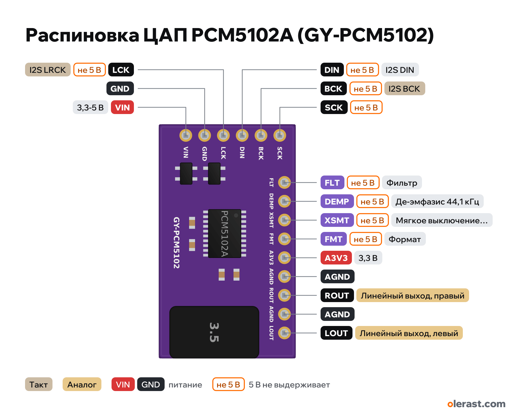
Top view, 6-pin connector on the left, 9-pin row on top, 3.5 mm jack on the right, rotated 90° on the diagram.
BuyDownload PNG- Chip
- TI PCM5102A
- Logic
- 3.3 V
- Power
- VIN 3.3-5 V
Important
- The back has 4 jumpers (1 FLT, 2 DEMP, 3 XSMT, 4 FMT) with H and L pads. Usual setting: 1L, 2L, 3H, 4L. On some boards they are not soldered: then there is no sound.
- SCK (MCLK) is not needed: tie it to GND with the jumper next to the pin, and the DAC takes its clock from BCK.
- Makerguides has FMT mixed up in the description: per the TI datasheet, low on FMT is I2S, high is left-justified.
- The output is line level (2.1 V RMS): to a speaker through an amplifier, to high-impedance headphones directly.
- Geometry from KiCad footprints (±0.2 mm), components drawn schematically.
Revisions and clones
- Blue CJMCU-5102 modules have a different pin order: check the labels.
- Modules with the PCM5102 (without the A) work the same way.
All pins
| Label | Number | Functions | Limits | Check |
|---|---|---|---|---|
| SCK | SCK: system clock (MCLK) | not 5 V tolerant | not from manufacturerNo-name module: labels and order from the symbol, two KiCad footprints and the Makerguides description (they agree), functions from the TI datasheet.Without MCLK tie it to GND (there is a jumper next to the pin on the front side): the chip derives the clock from BCK with its own PLL.3.3 V input (limit 3.9 V): from a 5 V Arduino only through a divider. | |
| BCK | I2S BCK: bit clock | not 5 V tolerant | not from manufacturerNo-name module: labels and order from the symbol, two KiCad footprints and the Makerguides description (they agree), functions from the TI datasheet.3.3 V input (limit 3.9 V): from a 5 V Arduino only through a divider.Labelled on other revisions as: BCLK | |
| DIN | I2S DIN: data | not 5 V tolerant | not from manufacturerNo-name module: labels and order from the symbol, two KiCad footprints and the Makerguides description (they agree), functions from the TI datasheet.3.3 V input (limit 3.9 V): from a 5 V Arduino only through a divider. | |
| LCK | I2S LRCK (WS): left or right channel | not 5 V tolerant | not from manufacturerNo-name module: labels and order from the symbol, two KiCad footprints and the Makerguides description (they agree), functions from the TI datasheet.3.3 V input (limit 3.9 V): from a 5 V Arduino only through a divider.Labelled on other revisions as: LRCK, LRC, WS | |
| GND | Ground | not from manufacturerNo-name module: labels and order from the symbol, two KiCad footprints and the Makerguides description (they agree), functions from the TI datasheet. | ||
| VIN | 5 V | power input | not from manufacturerNo-name module: labels and order from the symbol, two KiCad footprints and the Makerguides description (they agree), functions from the TI datasheet. | |
| FLT | Filter: low is normal latency, high is low latency | not 5 V tolerant | not from manufacturerNo-name module: labels and order from the symbol, two KiCad footprints and the Makerguides description (they agree), functions from the TI datasheet.Duplicates the jumper on the back: 1, default L. Don't use the pin and the jumper at the same time. | |
| DEMP | De-emphasis 44.1 kHz: low is off, high is on | not 5 V tolerant | not from manufacturerNo-name module: labels and order from the symbol, two KiCad footprints and the Makerguides description (they agree), functions from the TI datasheet.Duplicates the jumper on the back: 2, default L. Don't use the pin and the jumper at the same time.Labelled on other revisions as: DMP | |
| XSMT | Soft mute: low is silence, high is sound | not 5 V tolerant | not from manufacturerNo-name module: labels and order from the symbol, two KiCad footprints and the Makerguides description (they agree), functions from the TI datasheet.Duplicates the jumper on the back: 3, default H. Don't use the pin and the jumper at the same time.If jumper 3 on the board is not soldered and the pin is floating, there is no sound: solder 3H or apply a high level.Labelled on other revisions as: XMT, XMST | |
| FMT | Format: low is I2S, high is left-justified | not 5 V tolerant | not from manufacturerNo-name module: labels and order from the symbol, two KiCad footprints and the Makerguides description (they agree), functions from the TI datasheet.Duplicates the jumper on the back: 4, default L. Don't use the pin and the jumper at the same time. | |
| A3V3 | 3.3 V | power output | not from manufacturerNo-name module: labels and order from the symbol, two KiCad footprints and the Makerguides description (they agree), functions from the TI datasheet.Analog 3.3 V supply from the board's regulator. Don't load it. | |
| AGND | Ground | not from manufacturerNo-name module: labels and order from the symbol, two KiCad footprints and the Makerguides description (they agree), functions from the TI datasheet. | ||
| ROUT | Line output, right: up to 2.1 V RMS, centered on zero | not from manufacturerNo-name module: labels and order from the symbol, two KiCad footprints and the Makerguides description (they agree), functions from the TI datasheet.Output to an amplifier or high-impedance headphones; it can't drive a loud speaker. | ||
| AGND | Ground | not from manufacturerNo-name module: labels and order from the symbol, two KiCad footprints and the Makerguides description (they agree), functions from the TI datasheet. | ||
| LOUT | Line output, left: up to 2.1 V RMS, centered on zero | not from manufacturerNo-name module: labels and order from the symbol, two KiCad footprints and the Makerguides description (they agree), functions from the TI datasheet. |
Sources
Not verified against the manufacturer: 15 of 15 pins. The pin card says what confirms each one and where sources disagree.
- TI PCM5102A datasheet (SLAS859C)datasheet, checked 17.10.2026AVDD and CPVDD supply 3.0–3.6 V, digital inputs up to 3.9 V, XSMT (low is silence), FMT (low is I2S), FLT, DEMP, SCK to ground selects the internal PLL
- KiCad: gmcn42/clumsyMIDI GY-PCM5102 (symbol and footprint)third-party source, checked 17.10.202631.6×18.5, column SCK, BCK, DIN, LCK, GND, VIN 1.5 mm from the edge, row FLT, DEMP, XSMT, FMT, A3V3, AGND, ROUT, AGND, LOUT
- KiCad: polpo/picogus GY-PCM5102.kicad_modthird-party source, checked 17.10.2026same layout (second independent footprint), discrepancy up to 0.15 mm
- Makerguides: Playing audio with ESP32 and PCM5102third-party source, checked 17.10.20263.3–5 V supply, jumpers 1L 2L 3H 4L on the back, SCK jumper to ground, 3.5 mm jack duplicates the line output
Size: from KiCad footprints (clumsyMIDI 31.6×18.5; PicoGUS 31.8×18.8) (approximate).
FAQ
- What supply voltage does the GY-PCM5102 need?
- VIN: 3.3-5 V. 3.3 V logic.